
Voltage Regulator Module (VRM) and Enterprise Voltage Regulator-Down (EVRD) 10.0 Design Guidelines

VRM and EVRD 10.0 Design Guidelines
R
15
2.7 Dynamic Voltage Identification (VID) REQUIRED
VRM/EVRD 10.0 supports dynamic VID across the entire VID table, which requires the ability to
reduce the load line voltage shown in Figure 3 by 450 mV. The VRM/EVRD must be capable of
accepting voltage level changes of 12.5 mV steps every 5 µs, up to 36 steps (450 mV) in 180 µs.
The low voltage state will be maintained for at least 50 µs. The worst case settling time for the six
VID lines, including line-to-line skew, is 400 ns. The VID inputs should contain circuitry to
prevent false tripping or latching of VID codes during the settling time.
During a transition the output voltage must be between the maximum voltage of the high range
(“A” in Figure 7) and the minimum voltage of the low range (“B”). The VRM/EVRD must
respond to a transition from VID-low to VID-high by regulating its Vcc output to the range
defined by the new, final VID code within 50 µs of the final step. The time to move the output
voltage from VID-high to VID-low will depend on the PWM controller design, the amount of
system decoupling capacitance, and the processor load.
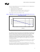
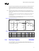
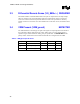
Figure 7 shows operating states as a representative processor changes levels. The diagram
assumes steady state, maximum current during the transition for ease of illustration; actual
processor behavior allows for any di/dt event during the transitions, depending on the code it is
executing at that time. In the example, the processor begins in a high load condition. In transitions
1→2 and 2→3, the processor prepares to switch to the low voltage range with a transition to a
low load condition, followed by an increased activity level. Transition 3→4 is a simplification of
the multiple steps from the high voltage load line to the low voltage load line. Transition 4→5 is
an example of a response to a load change during normal operation in the lower range.
Figure 7. Processor Transition States
VID High Load Line
1
2
3
4
Icc-max
5
VID Low Load Line
A
B
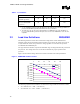
Figure 8 provides an illustration of dynamic VID. The diagram in Figure 8 assumes steady state,
constant current during the dynamic VID transition for ease of illustration; actual processor
behavior allows for any dIcc/dt during the transitions, depending on the code it is executing at
that time. Note that during dynamic VID, the processor will not output VID codes that would
disable the voltage regulator output voltage.
The processor load may not be sufficient to absorb all of the energy from the output capacitors on
the baseboard when VID changes to a lower output voltage. The VRM/EVRD design should
ensure that any energy transfer from the capacitors does not impair the operation of the
VRM/EVRD, the AC-DC supply, or any other parts of the system.