
Voltage Regulator Module (VRM) and Enterprise Voltage Regulator-Down (EVRD) 10.0 Design Guidelines


VRM and EVRD 10.0 Design Guidelines
R
3
Contents
1
Applications............................................................................................................... 8
1.1
Terminology.................................................................................................. 8
2
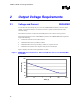
Output Voltage Requirements................................................................................. 10
2.1
Voltage and Current REQUIRED............................................................... 10
2.2
Load Line Definitions REQUIRED ............................................................. 12
2.3
Voltage Tolerance REQUIRED.................................................................. 13
2.4
Processor Vcc Overshoot REQUIRED ...................................................... 13
2.5
Stability REQUIRED...................................................................................14
2.6
Processor Power Sequencing REQUIRED ............................................... 14
2.7
Dynamic Voltage Identification (VID) REQUIRED ..................................... 15
2.8
Overshoot at Turn-On or Turn-Off REQUIRED ......................................... 16
2.9
Output Filter Capacitance REQUIRED ......................................................16
2.10
Shut-Down Response REQUIRED............................................................ 17
3
Control Signals........................................................................................................ 18
3.1
Output Enable (OUTEN) REQUIRED........................................................ 18
3.2
Voltage Identification (VID[5:0]) REQUIRED ............................................. 18
3.3
Differential Remote Sense (VO_SEN+/–) REQUIRED..............................20
3.4
VRM Present (VRM_pres#) EXPECTED...................................................20
4
Input Voltage and Current....................................................................................... 22
4.1
Input Voltages EXPECTED........................................................................ 22
4.2
Load Transient Effects on Input Current EXPECTED ...............................22
5
Processor Voltage Output Protection...................................................................... 24
5.1
Over-Voltage Protection (OVP) PROPOSED ............................................ 24
5.2
Over-Current Protection (OCP) PROPOSED ............................................ 24
6
Output Indicators..................................................................................................... 26
6.1
Vcc Power-Good (Vcc_PWRGD) PROPOSED ......................................... 26
6.2
Voltage Regulator Hot (VR_hot#) PROPOSED.........................................26
6.3
Load Indicator Output (Load_current) PROPOSED .................................. 27
6.4
VRM Identification (VRM_ID0, VRM_ID1) PROPOSED............................ 27
7
VRM – Mechanical Guidelines................................................................................ 28
7.1
VRM Connector EXPECTED ..................................................................... 28
7.2
VRM Connector Keying.............................................................................. 28
7.3
Pin Descriptions and Assignments ............................................................28
7.4
Mechanical Dimensions PROPOSED........................................................ 31
7.4.1
Gold Finger Specification ......................................................... 31
8
VRM – Environmental Conditions ........................................................................... 32