
Voltage Regulator Module (VRM) and Enterprise Voltage Regulator-Down (EVRD) 10.1 Design Guidelines


Voltage Regulator Module (VRM) and Enterprise Voltage 13
Regulator-Down (EVRD) 10.1 Design Guidelines
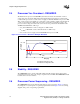
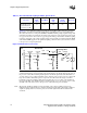
Output Voltage Requirements
NOTES:
1. V
TT
comes up at the application of system power to the Vtt VR. Vtt is used to supply VID [5:0] power to the
processor.
2. V
TT
VR generates VIDPWRGD after the VTT supply reaches 90% of the final value and must be a minimum
of 1 ms. It is used by the Vcc VR to latch the processor’s core VIDs outputs and should be a qualifier for
enabling the output of the Vcc VR.
3. Vcc_PWRGD is generated by the Vcc VR and may be used elsewhere in the system.
4. VIDPWRGD must deactivate and Vcc must be disabled immediately when Vtt becomes invalid.
5. Vcc_PWRGD should assert between 0 and 10 ms after Vcc reaches 90% of the final value.
6. See the processor datasheet for the latest timing requirements.
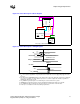
Figure 2-4. Power-On Sequence Block Diagram
Figure 2-5. Power-On Sequence Timing Diagram
CPU
VCC
VID[5:0]
Vcc VRM/EVRD
Vtt VR
Vcc
VID[5:0]
Vcc_PWRGD
OUTEN
VTT
VTT
VID_PWRGOOD
VIDPWRGD
To System
PWRGD
Delay *
* This Delay could be built into the V
TT
VR
OUTEN
2
Vcc
3, 5
Vcc_PWRGD
90% of Vcc
10ms MAX
Stage 2
1
Vtt
VIDPWRGD
2, 4
VID[5:0]
Valid
1
Not-Valid
90%
of Vtt
1ms<t
Vtt
<10ms
Stage 1
1
VIDs are valid as soon as
VIDPWRGD is active