
Voltage Regulator Module (VRM) and Enterprise Voltage Regulator-Down (EVRD) 10.1 Design Guidelines


VRM – Mechanical Guidelines
30 Voltage Regulator Module (VRM) and Enterprise Voltage
Regulator-Down (EVRD) 10.1 Design Guidelines
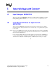
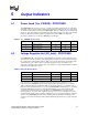
7.3 Pin Descriptions and Assignments
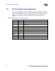
Table 7-2 shows the VRM10.1 connector pin description. The pins 4 and 59 labeled VIN+ and
VIN- are used on the VRM10.1 module as an additional input voltage pair. Those pins are labeled
“Reserved” in VRM10.0 and should not be used if there are plans to use VRM10.0 modules in this
connector. See the Voltage Regulator Module (VRM) and Enterprise Voltage Regulator-Down
(EVRD) 10.0 Design Guidelines for more information. The pin assignments are shown in
Table 7-3.
Table 7-2. VRM 10.1 Connector Pin Descriptions
Name Type Description
Load current Output Analog signal representing the output load current
OUTEN Input Output enable
Vcc_PWRGD Output Output signal indicating that the output voltage of the VRM is in the
specified range
VID [5:0] Input Voltage ID pins used to specify the VRM output voltage
VIN+ Power VRM Input Voltage
VIN− Ground VRM Input Ground
VO+ Power VRM Output Voltage
VO− Ground VRM Output Ground
VO_SEN+
VO_SEN–
Input Output voltage sense pins
VR_hot# Output Indicates to the system that a thermal event has been detected in the VR
VRM_pres# Output Indicates to the system that a VRM is plugged into the socket
LL0, LL1 Input Used to configure VR load line value