
VRM 9.1 DC-DC Converter Design Guidelines
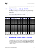
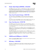
Table Of Contents
- 1 Electrical Specifications
- 1.1 Output Requirements
- 1.1.1 Voltage and Current - REQUIRED
- 1.1.2 Maximum Ratings - EXPECTED
- 1.1.3 Output Voltage Tolerance - REQUIRED
- 1.1.4 No-Load Operation - REQUIRED
- 1.1.5 Turn-on Response Time - EXPECTED
- 1.1.6 Overshoot and Undershoot at Turn-On or Turn-Off - REQUIRED
- 1.1.7 Converter Stability - REQUIRED
- 1.1.8 Current Sharing - REQUIRED
- 1.2 Input Voltage and Current
- 1.3 Control Inputs - REQUIRED
- 1.4 Remote Sense (VO-sen+, VO-sen-) - EXPECTED
- 1.5 Power Good Output (PWRGD) - REQUIRED
- 1.6 VRM Present (VRM-pres) - EXPECTED
- 1.7 Efficiency - PROPOSED
- 1.8 Isolation - PROPOSED
- 1.9 Fault Protection
- 1.1 Output Requirements
- 2 Module Layout Guidelines
- 3 Environmental Conditions
- 3.1 Operating Temperature - PROPOSED
- 3.2 VRM Board Temperature - REQUIRED
- 3.3 Non-Operating Temperature - PROPOSED
- 3.4 Humidity - PROPOSED
- 3.5 Altitude - PROPOSED
- 3.6 Electrostatic Discharge - PROPOSED
- 3.7 Shock and Vibration - PROPOSED
- 3.8 Electromagnetic Compatibility - PROPOSED
- 3.9 Reliability - PROPOSED
- 3.10 Safety - PROPOSED

Electrical Specifications
16 VRM 9.1 DC-DC Converter Design Guidelines
1.5 Power Good Output (PWRGD) - REQUIRED
The VRM must provide an open collector or equivalent Power Good signal consistent with TTL
DC levels. This signal should transition to the open (>100 kΩ) state within 10 ms of the output
voltage stabilizing within the range specified in Section 1.1.1. The signal should be in the low-
impedance (to ground) state whenever Vout
VRM
is outside of the required range below and be in
the open state whenever Vout
VRM
is within the range specified in Section 1.1.3. On power up, the
PWRGD signal must remain in the low-impedance state until the output voltage has stabilized
within the required tolerance.
1.5.1 Power Good Threshold Voltages - EXPECTED
The minimum voltage at which PWRGD is asserted should be the Vvrm
MIN
specified in
Section 1.1.3, minus margin to prevent false de-assertion, but at least 95% of (VID minus
125 mV).
The maximum voltage at which PWRGD is asserted should be the VID (set-point) voltage, plus
margin to prevent false de-assertion, but should be no greater than VID plus 250mV.
1.5.2 Power Good Operation - EXPECTED
This PWRGD output should be capable of sinking up to 4 mA, while maintaining a voltage of
0.4 V or lower. When the output is in the open state it should be capable of withstanding up to
5.5 V. Latch-up or damage cannot occur if the pull-up voltage on the system board is present with
no +12 V input present.
VRM Power Good should remain low if the VRM is disabled by the Output Enable pin. System
designers need to provide appropriate logic on the system board to decode VRM Power Good,
VRM Enable, and system Power Good to prevent a false not-good condition (Power Good = low)
when the VRM is disabled.
The VRM should be able to detect an internal failure and de-assert PWRGD even if the output is
within the defined PWRGD range. It is sufficient for this purpose to detect whether all phases are
switching at their output inductors. The intention of this provision is to detect failures
independently when VRMs are sharing current to a common power plane in a multiple-processor
system.
1.6 VRM Present (VRM-pres) - EXPECTED
This line is ground when the VRM is installed. The system board can use this signal to detect the
presence of each VRM installed in the system.
1.7 Efficiency - PROPOSED
The efficiency of the VRM should be greater than 80% at maximum output current. It should not
dissipate more power under any load condition than it does at maximum output current and
maximum input voltage.