
Intel Pentium M Processor on 90nm Process with 2-MB L2 Cache Datasheet

20 Datasheet
Electrical Specifications
NOTES:
1. Refer to Chapter 4 for signal descriptions and termination requirements.
2. BPM[2:0}# and PRDY# are AGTL+ output only signals.
3. In processor systems where there is no debug port implemented on the system board, these signals are used
to support a debug port interposer. In systems with the debug port implemented on the system board, these
signals are no connects.
3.7 CMOS Signals
CMOS input signals are shown in Table 3-2. Legacy output FERR#, IERR# and other non-AGTL+
signals (THERMTRIP# and PROCHOT#) utilize Open Drain output buffers. These signals do not
have setup or hold time specifications in relation to BCLK[1:0]. However, all of the CMOS signals
are required to be asserted for at least three BCLKs in order for the processor to recognize them.
See Section 3.9 for the DC and AC specifications for the CMOS signal groups.
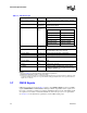
Table 3-2. FSB Pin Groups
Signal Group Type Signals
1
AGTL+ Common Clock Input Synchronous
to BCLK[1:0]
BPRI#, DEFER#, DPWR#, PREQ#, RESET#, RS[2:0]#,
TRDY#
AGTL+ Common Clock I/O Synchronous
to BCLK[1:0]
ADS#, BNR#, BPM[3:0]#, BR0#, DBSY#, DRDY#, HIT#,
HITM#, LOCK#, PRDY#
AGTL+ Source Synchronous I/O Synchronous
to assoc.
strobe
AGTL+ Strobes Synchronous
to BCLK[1:0]
ADSTB[1:0]#, DSTBP[3:0]#, DSTBN[3:0]#
CMOS Input Asynchronous A20M#, DPSLP#, IGNNE#, INIT#, LINT0/INTR, LINT1/
NMI, PWRGOOD, SMI#, SLP#, STPCLK#
Open Drain Output Asynchronous FERR#, IERR#, PROCHOT#, THERMTRIP#
CMOS Output Asynchronous PSI#, VID[5:0], BSEL[1:0]
CMOS Input Synchronous
to TCK
TCK, TDI, TMS, TRST#
Open Drain Output Synchronous
to TCK
TDO
FSB Clock Clock BCLK[1:0], ITP_CLK[1:0]
2
Power/Other COMP[3:0], DBR#
2
, GTLREF, RSVD, TEST2, TEST1,
THERMDA, THERMDC, V
CC
, V
CCA
[3:0], V
CCP,
V
CCQ
[1:0],
V
CC_SENSE
, V
SS,
V
SS_SENSE
Signals Associated Strobe
REQ[4:0]#, A[16:3]# ADSTB[0]#
A[31:17]# ADSTB[1]#
D[15:0]#, DINV0# DSTBP0#, DSTBN0#
D[31:16]#, DINV1# DSTBP1#, DSTBN1#
D[47:32]#, DINV2# DSTBP2#, DSTBN2#
D[63:48]#, DINV3# DSTBP3#, DSTBN3#