
Intel Pentium M Processor on 90nm Process with 2-MB L2 Cache Datasheet


Datasheet 45
Electrical Specifications
NOTES:
1. Unless otherwise noted, all specifications in this table apply to all processor frequencies.
2. V
IL is defined as the maximum voltage level at a receiving agent that will be interpreted as a logical low value.
3. V
IH is defined as the minimum voltage level at a receiving agent that will be interpreted as a logical high
value.
4. V
IH and VOH may experience excursions above VCCP. However, input signal drivers must comply with the
signal quality specifications in Chapter 3.
5. This is the pull down driver resistance. Refer to processor I/O buffer models for I/V characteristics. Measured
at 0.31*VCCP. R
ON
(min) = 0.38*R
TT,
R
ON
(typ) = 0.45*R
TT,
R
ON
(max) = 0.52*R
TT.
6. GTLREF should be generated from VCCP with a 1% tolerance resistor divider. The VCCP referred to in these
specifications is the instantaneous VCCP.
7. R
TT
is the on-die termination resistance measured at V
OL
of the AGTL+ output driver. Measured at
0.31*VCCP. R
TT
is connected to VCCP on die. Refer to processor I/O buffer models for I/V characteristics.
8. Specified with on die R
TT
and R
ON
are turned off.
9. Cpad includes die capacitance only. No package parasitics are included.
NOTES:
1. Unless otherwise noted, all specifications in this table apply to all processor frequencies.
2. The VCCP referred to in these specifications refers to instantaneous VCCP.
3. Refer to the processor I/O buffer models for I/V characteristics.
4. Measured at 0.1*VCCP.
5. Measured at 0.9*VCCP.
6. For Vin between 0 V and VCCP. Measured when the driver is tristated.
7. Cpad includes die capacitance only. No package parasitics are included
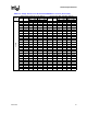
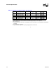
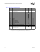
Table 3-23. AGTL+ Signal Group DC Specifications
Symbol Parameter Min Typ Max Unit Notes
1
VCCP I/O Voltage 0.997 1.05 1.102 V
GTLREF Reference Voltage 2/3 VCCP -
2%
2/3 VCCP 2/3 VCCP +
2%
V6
V
IH Input High Voltage GTLREF+0.1 VCCP+0.1 V 3,6
V
IL Input Low Voltage -0.1 GTLREF-0.1 V 2,4
V
OH Output High Voltage VCCP 6
R
TT
Termination Resistance 47 55 63 7
R
ON Buffer On Resistance 17.7 24.7 32.9
5
I
LI Input Leakage Current ± 100 µA 8
Cpad Pad Capacitance 1.8 2.3 2.75 pF 9
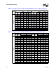
Table 3-24. CMOS Signal Group DC Specifications
Symbol Parameter Min Typ Max Unit Notes
1
VCCP I/O Voltage 0.997 1.05 1.102 V
V
IL Input Low Voltage
CMOS
-0.1 0.3*VCCP V 2, 3
V
IH Input High Voltage 0.7*VCCP VCCP+0.1 V 2
V
OL Output Low Voltage -0.1 0 0.1*VCCP V 2
V
OH Output High Voltage 0.9*VCCP VCCP VCCP+0.1 V 2
I
OL Output Low Current 1.49 4.08 mA 4
I
OH Output High Current 1.49 4.08 mA 5
I
LI
Leakage Current ± 100 µA 6
Cpad Pad Capacitance 1.0 2.3 3.0 pF