
Intel Pentium M Processor on 90nm Process with 2-MB L2 Cache Datasheet


Package Mechanical Specifications and Pin Information
Datasheet 65
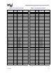
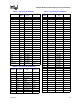
AD23 D[54]# Source Synch Input/Output
AD24 D[57]# Source Synch Input/Output
AD25 VSS Power/Other
AD26 GTLREF Power/Other
AE1 A[30]# Source Synch Input/Output
AE2 A[27]# Source Synch Input/Output
AE3 VSS Power/Other
AE4 A[22]# Source Synch Input/Output
AE5 ADSTB[1]# Source Synch Input/Output
AE6 VSS Power/Other
AE7 VCCSENSE Power/Other Output
AE8 VSS Power/Other
AE9 VCC Power/Other
AE10 VSS Power/Other
AE11 VCC Power/Other
AE12 VSS Power/Other
AE13 VCC Power/Other
AE14 VSS Power/Other
AE15 VCC Power/Other
AE16 VSS Power/Other
AE17 VCC Power/Other
AE18 VSS Power/Other
AE19 VCC Power/Other
AE20 VSS Power/Other
AE21 D[59]# Source Synch Input/Output
AE22 D[55]# Source Synch Input/Output
AE23 VSS Power/Other
AE24 DSTBN[3]# Source Synch Input/Output
AE25 DSTBP[3]# Source Synch Input/Output
AE26 VSS Power/Other
AF1 A[31]# Source Synch Input/Output
AF2 VSS Power/Other
AF3 A[29]# Source Synch Input/Output
AF4 A[17]# Source Synch Input/Output
AF5 VSS Power/Other
AF6 VSSSENSE Power/Other Output
AF7 RSVD Reserved
AF8 VCC Power/Other
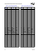
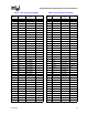
Table 4-4. Pin Listing by Pin Number
Pin
Number
Pin Name
Signal Buffer
Type
Direction
AF9 VSS Power/Other
AF10 VCC Power/Other
AF11 VSS Power/Other
AF12 VCC Power/Other
AF13 VSS Power/Other
AF14 VCC Power/Other
AF15 VSS Power/Other
AF16 VCC Power/Other
AF17 VSS Power/Other
AF18 VCC Power/Other
AF19 VSS Power/Other
AF20 D[58]# Source Synch Input/Output
AF21 VSS Power/Other
AF22 D[62]# Source Synch Input/Output
AF23 D[56]# Source Synch Input/Output
AF24 VSS Power/Other
AF25 D[61]# Source Synch Input/Output
AF26 D[63]# Source Synch Input/Output
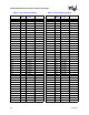
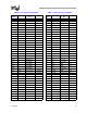
B1 VCCA[1] Power/Other
B2 RSVD Reserved
B3 VSS Power/Other
B4 SMI# CMOS Input
B5 INIT# CMOS Input
B6 VSS Power/Other
B7 DPSLP# CMOS Input
B8 BPM[1]# Common Clock Output
B9 VSS Power/Other
B10 PREQ# Common Clock Input
B11 RESET# Common Clock Input
B12 VSS Power/Other
B13 TRST# CMOS Input
B14 BCLK[1] Bus Clock Input
B15 BCLK[0] Bus Clock Input
B16 VSS Power/Other
B17 PROCHOT# Open Drain Output
B18 THERMDA Power/Other
B19 VSS Power/Other
B20 D[7]# Source Synch Input/Output
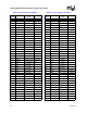
Table 4-4. Pin Listing by Pin Number
Pin
Number
Pin Name
Signal Buffer
Type
Direction