
Intel Pentium M Processor on 90nm Process with 2-MB L2 Cache Datasheet


Package Mechanical Specifications and Pin Information
Datasheet 69
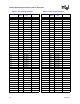
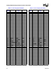
T25 D[34]# Source Synch Input/Output
T26 VSS Power/Other
U1 A[13]# Source Synch Input/Output
U2 VSS Power/Other
U3 ADSTB[0]# Source Synch Input/Output
U4 A[4]# Source Synch Input/Output
U5 VCC Power/Other
U6 VSS Power/Other
U21 VCCP Power/Other
U22 VSS Power/Other
U23 D[35]# Source Synch Input/Output
U24 VSS Power/Other
U25 D[43]# Source Synch Input/Output
U26 D[41]# Source Synch Input/Output
V1 VSS Power/Other
V2 A[7]# Source Synch Input/Output
V3 A[5]# Source Synch Input/Output
V4 VSS Power/Other
V5 VSS Power/Other
V6 VCC Power/Other
V21 VSS Power/Other
V22 VCC Power/Other
V23 D[36]# Source Synch Input/Output
V24 D[42]# Source Synch Input/Output
V25 VSS Power/Other
V26 D[44]# Source Synch Input/Output
W1 A[8]# Source Synch Input/Output
W2 A[10]# Source Synch Input/Output
W3 VSS Power/Other
W4 VCCQ[1] Power/Other
W5 VCC Power/Other
W6 VSS Power/Other
W21 VCC Power/Other
W22 VSS Power/Other
W23 VSS Power/Other
W24 DSTBP[2]# Source Synch Input/Output
W25 DSTBN[2]# Source Synch Input/Output
W26 VSS Power/Other
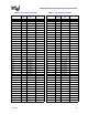
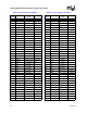
Table 4-4. Pin Listing by Pin Number
Pin
Number
Pin Name
Signal Buffer
Type
Direction
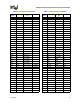
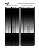
Y1 A[12]# Source Synch Input/Output
Y2 VSS Power/Other
Y3 A[15]# Source Synch Input/Output
Y4 A[11]# Source Synch Input/Output
Y5 VSS Power/Other
Y6 VCC Power/Other
Y21 VSS Power/Other
Y22 VCC Power/Other
Y23 D[45]# Source Synch Input/Output
Y24 VSS Power/Other
Y25 D[47]# Source Synch Input/Output
Y26 D[32]# Source Synch Input/Output
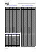
Table 4-4. Pin Listing by Pin Number
Pin
Number
Pin Name
Signal Buffer
Type
Direction