
Datasheet


ELECTRICAL SPECIFICATIONS
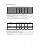
25
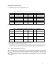
Table 12. System Bus AC Specifications (Clock)
at the processor Core Pins
1, 2, 3
T# Parameter Min Nom Max Unit Figure Notes
System Bus Frequency
90
100.2
MHz
4
T1: BCLK Period 10.0 11.11 nS
4 4, 5, 9
T2: BCLK Period Stability ±150 pS 6, 7, 9
T3: BCLK High Time 2.5 nS 4, 12 @>2.0V, 9
T4: BCLK Low Time 2.5 nS 4, 12 @<0.5V, 9
T5: BCLK Rise Time 0.50 1.5 nS 4, 12 0.5V–2.0V 8, 9
T6: BCLK Fall Time 0.50 1.5 nS 4, 12 2.0V–0.5V 8
,
9
NOTES:
1. Unless otherwise noted, all specifications in this table apply to all processor frequencies and cache sizes.
2. All AC timings for the AGTL+ signals are referenced to the BCLK rising edge at 1.25V at the processor core pin. All AGTL+ signal
timings (address bus, data bus, etc.) are referenced at 1.00V at the processor core pins.
3. All AC timings for the CMOS signals are referenced to the BCLK rising edge at 1.25V at the processor core pin. All CMOS signal
timings (compatibility signals, etc.) are referenced at 1V at the processor core pins.
4. The internal core clock frequency is derived from the processor system bus clock. The system bus clock to core clock ratio is
determined during initialization as described in 6.2. Table 1 shows the supported ratios for each processor.
5. The BCLK period allows a +0.5 nS tolerance for clock driver variation. See the CK98WS Clock Synthesizer/Driver Specification for
further information.
6. Due to the difficulty of accurately measuring clock jitter in a system, it is recommended that a clock driver be used that is designed to
meet the period stability specification into a test load of 10 to 20 pF. This should be measured on the rising edges of adjacent BCLKs
crossing 1.25V at the processor core pin. The jitter present must be accounted for as a component of BCLK timing skew between
devices.
7. The clock driver’s closed loop jitter bandwidth must be set low to allow any PLL-based device to track the jitter created by the clock
driver. The –20 dB attenuation point, as measured into a 10 to 20 pF load, should be less than 500 kHz. This specification may be
ensured by design characterization and/or measured with a spectrum analyzer. See the CK98WS Clock Synthesizer/Driver
Specification for further details.
8. Not 100% tested. Specified by design characterization as a clock driver requirement.
9. This frequency range is specified by the CK98WS Clock Synthesizer/Driver Specification, and is guaranteed by design only (not
tested).