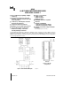
8086 16-BIT HMOS MICROPROCESSOR 8086/8086-2/8086-1 Y Direct Addressing Capability 1 MByte of Memory Y Architecture Designed for Powerful Assembly Language and Efficient High Level Languages Y 14 Word, by 16-Bit Register Set with Symmetrical Operations Y 24 Operand Addressing Modes Y Bit, Byte, Word, and Block Operations Y 8 and 16-Bit Signed and Unsigned Arithmetic in Binary or Decimal Including Multiply and Divide Y Range of Clock Rates: 5 MHz for 8086, 8 MHz for 8086-2, 10 MHz for 8086-1 Y
8086 Table 1. Pin Description The following pin function descriptions are for 8086 systems in either minimum or maximum mode. The ‘‘Local Bus’’ in these descriptions is the direct multiplexed bus interface connection to the 8086 (without regard to additional bus buffers). Symbol Pin No. Type Name and Function AD15 –AD0 2–16, 39 I/O ADDRESS DATA BUS: These lines constitute the time multiplexed memory/IO address (T1), and data (T2, T3, TW, T4) bus.
8086 Table 1. Pin Description (Continued) Symbol Pin No. Type Name and Function READY 22 I READY: is the acknowledgement from the addressed memory or I/O device that it will complete the data transfer. The READY signal from memory/IO is synchronized by the 8284A Clock Generator to form READY. This signal is active HIGH. The 8086 READY input is not synchronized. Correct operation is not guaranteed if the setup and hold times are not met.
8086 Table 1. Pin Description (Continued) Symbol Pin No. Type Name and Function S2, S1, S0 (Continued) 26–28 O These signals float to 3-state OFF in ‘‘hold acknowledge’’. These status lines are encoded as shown.
8086 Table 1. Pin Description (Continued) Symbol Pin No. Type Name and Function QS1, QS0 24, 25 O QUEUE STATUS: The queue status is valid during the CLK cycle after which the queue operation is performed. QS1 and QS0 provide status to allow external tracking of the internal 8086 instruction queue.
8086 bytes, addressed as 00000(H) to FFFFF(H). The memory is logically divided into code, data, extra data, and stack segments of up to 64K bytes each, with each segment falling on 16-byte boundaries. (See Figure 3a.) FUNCTIONAL DESCRIPTION General Operation The internal functions of the 8086 processor are partitioned logically into two processing units. The first is the Bus Interface Unit (BIU) and the second is the Execution Unit (EU) as shown in the block diagram of Figure 1.
8086 address FFFF0H through FFFFFH are reserved for operations including a jump to the initial program loading routine. Following RESET, the CPU will always begin execution at location FFFF0H where the jump must be. Locations 00000H through 003FFH are reserved for interrupt operations. Each of the 256 possible interrupt types has its service routine pointed to by a 4-byte pointer element consisting of a 16-bit segment address and a 16-bit offset address.
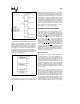
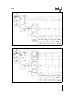
086 231455 – 5 Figure 4a. Minimum Mode 8086 Typical Configuration 231455 – 6 Figure 4b.
8086 can occur between 8086 bus cycles. These are referred to as ‘‘Idle’’ states (Ti) or inactive CLK cycles. The processor uses these cycles for internal housekeeping. During T1 of any bus cycle the ALE (Address Latch Enable) signal is emitted (by either the processor or the 8288 bus controller, depending on the MN/MX strap). At the trailing edge of this pulse, a valid address and certain status information for the cycle may be latched.
8086 Status bits S3 through S7 are multiplexed with highorder address bits and the BHE signal, and are therefore valid during T2 through T4. S3 and S4 indicate which segment register (see Instruction Set description) was used for this bus cycle in forming the address, according to the following table: S4 S3 Characteristics 0 (LOW) 0 Alternate Data (extra segment) 0 1 Stack 1 (HIGH) 0 Code or None 1 1 Data NMI asserted prior to the 2nd clock after the end of RESET will not be honored.
8086 MASKABLE INTERRUPT (INTR) HALT The 8086 provides a single interrupt request input (INTR) which can be masked internally by software with the resetting of the interrupt enable FLAG status bit. The interrupt request signal is level triggered. It is internally synchronized during each clock cycle on the high-going edge of CLK. To be responded to, INTR must be present (HIGH) during the clock period preceding the end of the current instruction or the end of a whole move for a blocktype instruction.
8086 EXTERNAL SYNCHRONIZATION VIA TEST SYSTEM TIMINGÐMINIMUM SYSTEM As an alternative to the interrupts and general I/O capabilities, the 8086 provides a single softwaretestable input known as the TEST signal. At any time the program may execute a WAIT instruction. If at that time the TEST signal is inactive (HIGH), program execution becomes suspended while the processor waits for TEST to become active. It must remain active for at least 5 CLK cycles.
8086 lines D7 –D0 as supplied by the inerrupt system logic (i.e., 8259A Priority Interrupt Controller). This byte identifies the source (type) of the interrupt. It is multiplied by four and used as a pointer into an interrupt vector lookup table, as described earlier.
8086 ABSOLUTE MAXIMUM RATINGS* NOTICE: This is a production data sheet. The specifications are subject to change without notice. Ambient Temperature Under Bias ÀÀÀÀÀÀ0§ C to 70§ C Storage Temperature ÀÀÀÀÀÀÀÀÀÀ b 65§ C to a 150§ C Voltage on Any Pin with Respect to GroundÀÀÀÀÀÀÀÀÀÀÀÀÀÀ b 1.0V to a 7V Power DissipationÀÀÀÀÀÀÀÀÀÀÀÀÀÀÀÀÀÀÀÀÀÀÀÀÀÀ2.5W D.C. CHARACTERISTICS Symbol *WARNING: Stressing the device beyond the ‘‘Absolute Maximum Ratings’’ may cause permanent damage.
8086 A.C.
8086 A.C.
8086 A.C. TESTING INPUT, OUTPUT WAVEFORM A.C. TESTING LOAD CIRCUIT 231455-11 A.C. Testing: Inputs are driven at 2.4V for a Logic ‘‘1’’ and 0.45V for a Logic ‘‘0’’. Timing measurements are made at 1.5V for both a Logic ‘‘1’’ and ‘‘0’’.
8086 WAVEFORMS (Continued) MINIMUM MODE (Continued) 231455 – 14 SOFTWARE HALTÐ RD, WR, INTA e VOH DT/R e INDETERMINATE NOTES: 1. All signals switch between VOH and VOL unless otherwise specified. 2. RDY is sampled near the end of T2, T3, TW to determine if TW machines states are to be inserted. 3. Two INTA cycles run back-to-back. The 8086 LOCAL ADDR/DATA BUS is floating during both INTA cycles. Control signals shown for second INTA cycle. 4. Signals at 8284A are shown for reference only. 5.
8086 A.C. CHARACTERISTICS MAX MODE SYSTEM (USING 8288 BUS CONTROLLER) TIMING REQUIREMENTS Symbol 8086 Parameter 8086-1 8086-2 Min Max Min Max Min Max 500 100 500 125 500 Units TCLCL CLK Cycle Period 200 TCLCH CLK Low Time 118 53 68 ns TCHCL CLK High Time 69 39 44 ns Test Conditions ns TCH1CH2 CLK Rise Time 10 10 10 ns From 1.0V to 3.5V TCL2CL1 CLK Fall Time 10 10 10 ns From 3.5V to 1.
8086 A.C.
8086 A.C.
8086 WAVEFORMS MAXIMUM MODE 231455 – 15 22
8086 WAVEFORMS (Continued) MAXIMUM MODE (Continued) 231455 – 16 NOTES: 1. All signals switch between VOH and VOL unless otherwise specified. 2. RDY is sampled near the end of T2, T3, TW to determine if TW machines states are to be inserted. 3. Cascade address is valid between first and second INTA cycle. 4. Two INTA cycles run back-to-back. The 8086 LOCAL ADDR/DATA BUS is floating during both INTA cycles. Control for pointer address is shown for second INTA cycle. 5.
8086 WAVEFORMS (Continued) ASYNCHRONOUS SIGNAL RECOGNITION 231455 – 17 NOTE: 1. Setup requirements for asynchronous signals only to guarantee recognition at next CLK. BUS LOCK SIGNAL TIMING (MAXIMUM MODE ONLY) RESET TIMING 231455 – 18 231455 – 19 REQUEST/GRANT SEQUENCE TIMING (MAXIMUM MODE ONLY) 231455 – 20 NOTE: The coprocessor may not drive the buses outside the region shown without risking contention.
8086 WAVEFORMS (Continued) HOLD/HOLD ACKNOWLEDGE TIMING (MINIMUM MODE ONLY) 231455 – 21 25
8086 Table 2.
8086 Table 2. Instruction Set Summary (Continued) Mnemonic and Description ARITHMETIC Instruction Code 76543210 76543210 76543210 76543210 data if s: w e 01 ADD e Add: Reg./Memory with Register to Either 000000dw mod reg r/m Immediate to Register/Memory 100000sw mod 0 0 0 r/m data Immediate to Accumulator 0000010w data data if w e 1 ADC e Add with Carry: Reg.
8086 Table 2.
8086 Table 2.
8086 Table 2.