
Express Chipset Development Kit User's Manual

Mobile Intel
®
915GME Express Chipset —Hardware Reference
Mobile Intel
®
915GME Express Chipset
Development Kit User’s Manual April 2007
38 Order Number: 317230-001US
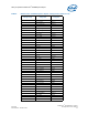
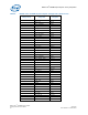
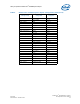
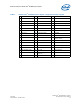
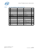
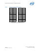
Table 8. Supported Configuration Jumper/Switch Settings
No. Default Setting Optional Setting Option Setting
Ref.
Desig.
1 SIO Reset 1-2 Normal Operation 2-3 to hold the SIO in Reset J7E4
2 H8 Reset 1-2 Normal Operation 2-3 to hold the H8 in Reset J8G1
3 1 Hz Clock Out - Normal Operation
IN - Clock disabled- enable H8
Programming
J9G1
4 H8 Programming OUT - Normal Operation
In - Enable external H8
Programming.
J9J3
5 LID Switch 1-2 Normal Operation 2-3 LID Switch Closed SW9J2
6 H8 Disable OUT - Normal Operation 1-2 disable the H8 J9J1
7 BIOS Recovery OUT - Normal Operation IN - Recover BIOS J8H2
8 In-Circuit H8 Programming 1-2 Normal Operation 2-3 to program the H8 J7J1
9 Clear CMOS OUT - Normal operation In to clear J6H1
10 Force Shutdown OUT - Normal operation
IN to force the board to
shutdown.
J2H1
13 Thermal Diode Connection 1-2 Normal Operation
Empty - Disable the processor
thermal diode from ADM1023
J3B3
14 Sleep S3 Hot/Cold Switch 1-2 S3_HOT 2-3 S3_COLD SW4A1
15 Tx Select 1-2 Normal Operation
2-3 connect TxD to H8 for
programming
J7A3
16 Rx Select 1-2 Normal Operation
2-3 connect RxD to H8 for
programming
J7A2