
Datasheet


Intel
®
Xeon
®
Processor C5500/C3500 Series
February 2010 Datasheet, Volume 1
Order Number: 323103-001 297
PCI Express Non-Transparent Bridge
3.21.1.24 WCCNTRL: Write Cache Control Register
This register is used for IIO write cache controlability
3.21.1.25 B2BSPAD[0 - 15]: Back-to-back Scratchpad Registers 0 - 15
These registers are valid when in NTB/NTB configuration. This set of 16 registers,
B2BSPAD0 through B2BSPAD15, is used by the processor on the Primary side of the
NTB to generate accesses to the Scratchpad registers on a second NTB whose
Secondary side is connected to the Secondary side of this NTB. Writing to these
registers will cause the NTB to generate a PCIe packet that is sent to the connected
NTB’s Scratchpad registers. This mechanism allows inter-system communication
through the pair of NTBs. The B2BBAR0XLAT register must be properly configured to
point to BAR 0/1 on the opposite NTB for this mechanism to function properly. This
mechanism doesn’t require a semaphore because each NTB has a set of Scratchpad
registers. The system passing information will always write to the registers on the
opposite NTB, and read its own Scratchpad registers to get information from the
opposite system.
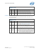
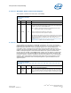
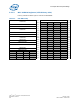
Register:WCCNTRL
Bar:PB01BASE, SB01BASE
Offset:E0h
Bit Attr Default Description
31:01 RO 0h Reserved
00 RW1S 0b
WCFLUSH
When set forces snap shot flush of the IIO write cache. This register can be
set either by host write or inbound MMIO write.
Note: This bit is cleared by hardware upon completion of write cache
flush. Software cannot clear this register.
1 = Force snap shot flush of entire IIO write cache
0 = No flush requested or flush operation complete
Usage model for this register is such that only a single flush can be issued at
a time until acknowledge of completion is received. Writing bit to 1 while it is
already set will not cause an additional flush. Flush will only occur on
transition from 0 to 1.
See Section 26.7.4.1, “ADR Write Cache (WC) flush acknowledge example
using NTB/NTB” for details on how to utilize this register.
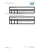
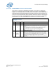
Register:B2BSPADn
Bar:PB01BASE, SB01BASE
Offset:100h, 104h, 108h, 10Ch, 110h, 114h, 118h, 11Ch, 120h, 124h, 128h, 12Ch, 130h, 134h,
138h, 13Ch
Bit Attr Default Description
31:0
Bar: Attr
PB01BASE:
RW
else: RO
00h
Back-to-back Scratchpad Register n
This set of 16 registers is written only from the Primary side of the NTB. A
write to any of these registers will cause the NTB to generate a PCIe packet
which is sent across the link to the opposite NTB’s corresponding Scratchpad
register.