
Datasheet

Datasheet 19
Intel
®
Celeron
®
Processor up to 1.10 GHz
The PPGA package has more power (88) and ground (80) pins than the S.E.P. Package. Of the
power pins, 77 are used for the processor core (V
CC
CORE
) and 8 are used as a AGTL+ reference
voltage (V
REF). The other 3 power pins are VCC
1.5
, VCC
2.5
and VCC
CMOS
and are used for future
processor compatibility.
FC-PGA/FC-PGA2 packages have 77 V
CC
CORE
, 77 ground pins, eight VREF, one VCC
1.5
, one
V
CC
2.5
, and one VCC
CMOS
. VCC
CORE
inputs supply the processor core, including the on-die L2
cache. The V
REF inputs are used as the AGTL+ reference voltage for the processor.
The V
CC
CMOS
pin is provided as a feature for future processor support in a flexible design. In such
a design, the V
CC
CMOS
pin is used to provide the CMOS voltage for use by the platform.
Additionally, 2.5 V must be provided to the V
CC
2.5
input and 1.5 V must be provided to the Vcc
1.5
input. The processor routes the CMOS voltage level through the package that it is compatible with.
For example, processors requiring 1.5 V CMOS voltage levels route 1.5 V to the V
CC
CMOS
output.
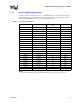
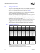
Each power signal, regardless of package, must meet the specifications stated in Table 4. In
addition, all V
CC
CORE
pins must be connected to a voltage island while all VSS pins have to
connect to a system ground plane. In addition, the motherboard must implement the V
TT pins as a
voltage island or large trace. Similarly, all V
SS pins must be connected to a system ground plane.
2.3.1 Phase Lock Loop (PLL) Power
It is highly critical that phase lock loop power delivery to the processor meets Intel’s requirements.
A low pass filter is required for power delivery to pins PLL1 and PLL2. This serves as an isolated,
decoupled power source for the internal PLL.
2.4 Processor Decoupling
Due to the large number of transistors and high internal clock speeds, the processor is capable of
generating large average current swings between low and full power states. This causes voltages on
power planes to sag below their nominal values if bulk decoupling is not adequate. Care must be
taken in the board design to ensure that the voltage provided to the processor remains within the
specifications listed in Table 5. Failure to do so can result in timing violations or a reduced lifetime
of the component.
2.4.1 System Bus AGTL+ Decoupling
The S.E.P. Package and FC-PGA/FC-PGA2 packages contain high frequency decoupling
capacitance on the processor substrate, where the PPGA package does not. Therefore, Celeron
processors in the PGA packages require high frequency decoupling on the system motherboard.
Bulk decoupling must be provided on the motherboard for proper AGTL+ bus operation for all
packages. See AP-585, Pentium
®
II Processor AGTL+ Guidelines (Order Number 243330), AP-
587, Pentium
®
II Processor Power Distribution Guidelines (Order Number 243332), and the
Pentium
®
II Processor Developer's Manual (Order Number 243502) for more information.