
Datasheet

40 Datasheet
Intel
®
Celeron
®
Processor up to 1.10 GHz
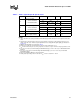
NOTES:
1. Unless otherwise noted, all specifications in this table apply to all processor frequencies.
2. These specifications are tested during manufacturing.
3. All AC timings for the AGTL+ signals are
REFerenced to the BCLK rising edge at 1.25 V at the processor pin.
All GTL+ signal timings (compatibility signals, etc.) are referenced at 1.00 V at the processor pins.
4. This specification applies to the processor operating with a 66 MHz system bus only.
5. Valid delay timings for these signals are specified into 25 Ω to 1.5 V and with V
REF at 1.0 V.
6. A minimum of 3 clocks must be guaranteed between two active-to-inactive transitions of TRDY#.
7. RESET# can be asserted (active) asynchronously, but must be deasserted synchronously.
8. After V
CC
CORE
and BCLK become stable.
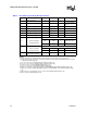
NOTES:
1. Unless otherwise noted, all specifications in this table apply to all Celeron processors at all frequencies and
cache sizes.
2. These specifications are tested during manufacturing.
3. All AC timings for the AGTL+ signals are referenced to the BCLK rising edge at 1.25 V at the processor pin.
All AGTL+ signal timings (compatibility signals, etc.) are referenced at 1.00V at the processor pins.
4. Valid delay timings for these signals are specified into 50 Ω to 1.5 V and with V
REF at 1.0 V.
5. A minimum of 3 clocks must be guaranteed between two active-to-inactive transitions of TRDY#.
6. RESET# can be asserted (active) asynchronously, but must be deasserted synchronously.
7. Specification is for a minimum 0.40 V swing from V
REF - 200 mV to VREF + 200 mV. This assumes an edge
rate of 0.3 V/ns.
8. Specification is for a maximum 1.0 V swing from V
TT – 1V to VTT. This assumes an edge rate of 3 V/ns.
9. This should be measured after V
CC
CORE
, VCC
CMOS
, and BCLK become stable.
10.This specification applies to the FC-PGA/FC-PGA2 packages running at 66 MHz system bus frequency.
11.This specification applies to the FC-PGA/FC-PGA2 packages running at 100 MHz system bus frequency.
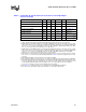
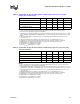
Table 15. Processor System Bus AC Specifications (AGTL+ Signal Group) at the Processor
Core Pins (for PPGA Package)
T# Parameter Min Max Unit Figure Notes
T7: AGTL+ Output Valid Delay 0.30 4.43 ns 4 5
T8: AGTL+ Input Setup Time 2.10 ns 5 5, 6, 7
T9: AGTL+ Input Hold Time 0.85 ns 5
T10: RESET# Pulse Width 1.00 ms 6 7, 8
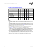
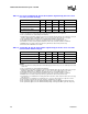
Table 16. System Bus AC Specifications (AGTL+ Signal Group) at the Processor Core Pins
(for FC-PGA/FC-PGA2 Packages)
T# Parameter Min Max Unit Figure Notes
T7: AGTL+ Output Valid Delay 0.40 3.25 ns 4 4, 10, 11
T8: AGTL+ Input Setup Time 1.20 ns 5 5, 6, 7, 10, 11
T9: AGTL+ Input Hold Time 1.00 ns 5 8, 10, 11
T10: RESET# Pulse Width 1.00 ms 7 6, 9, 10, 11