
Datasheet


Datasheet 41
Intel
®
Celeron
®
Processor up to 1.10 GHz
NOTES:
1. Unless otherwise noted, all specifications in this table apply to all Celeron processor frequencies.
2. Not 100% tested. Specified by design characterization.
3. All AC timings for the CMOS signals are referenced to the BCLK rising edge at 0.50 V at the processor edge
fingers. All CMOS signal timings (address bus, data bus, etc.) are referenced at 1.25 V.
4. These signals may be driven asynchronously.
5. This specification only applies when the APIC is enabled and the LINT1 or LINT0 pin is configured as an
edge-triggered interrupt with fixed delivery; otherwise, specification T14 applies.
PWRGOOD must remain below V
IL,max
(Table 6) until all the voltage planes meet the voltage tolerance
specifications in Table 5 and BCLK has met the BCLK AC specifications in Table 10 for at least 10 clock
cycles. PWRGOOD must rise glitch-free and monotonically to 2.5 V.
6. When driven inactive or after V
CC
CORE
, and BCLK become stable.
7. If the BCLK signal meets its AC specification within 150 ns of turning on, then the PWRGOOD inactive pulse
width specification (T15) is waived and BCLK may start after PWRGOOD is asserted. PWRGOOD must still
remain below V
IL,max
until all the voltage planes meet the voltage tolerance specifications.
NOTES:
1. Unless otherwise noted, all specifications in this table apply to all Celeron processor frequencies.
2. These specifications are tested during manufacturing.
3. All AC timings for the CMOS signals are referenced to the BCLK rising edge at 1.25 V at the processor core
pins. All CMOS signal timings (address bus, data bus, etc.) are referenced at 1.25 V.
4. These signals may be driven asynchronously.
5. This specification only applies when the APIC is enabled and the LINT1 or LINT0 pin is configured as an
edge-triggered interrupt with fixed delivery; otherwise, specification T14 applies.
6. When driven inactive or after V
CC
CORE
, and BCLK become stable.
7. If the BCLK signal meets its AC specification within 150 ns of turning on, then the PWRGOOD inactive pulse
width specification (T15) is waived and BCLK may start after PWRGOOD is asserted. PWRGOOD must still
remain below V
IL,max
until all the voltage planes meet the voltage tolerance specifications.
PWRGOOD must remain below V
IL,max
(Table 6) until all the voltage planes meet the voltage tolerance
specifications in Table 5 and BCLK has met the BCLK AC specifications in Table 10 for at least 10 clock
cycles. PWRGOOD must rise glitch-free and monotonically to 2.5 V.
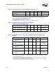
Table 17. System Bus AC Specifications (CMOS Signal Group) at the Processor Edge Fingers
(for S.E.P. Package)
T# Parameter Min Max Unit Figure Notes
T14’: CMOS Input Pulse Width, except
PWRGOOD
2BCLKs8
Active and
Inactive states
T14B: LINT[1:0] Input Pulse Width 6 BCLKs 8 5
T15’: PWRGOOD Inactive Pulse Width 10 BCLKs 8 6, 7
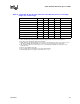
Table 18. System Bus AC Specifications (CMOS Signal Group) at the Processor Core Pins
(for Both S.E.P., PGA, and FC-PGA/FC-PGA2 Packages)
T# Parameter Min Max Unit Figure Notes
T14: CMOS Input Pulse Width, except
PWRGOOD
2BCLKs8
Active and
Inactive states
T14B: LINT[1:0] Input Pulse Width
(S.E.P.P. Only)
6BCLKs8 5
T15: PWRGOOD Inactive Pulse Width 10 BCLKs 8 6, 7