
Datasheet

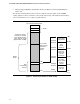
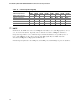

Table Of Contents
- Intel® Desktop Boards D915GEV/D915GRF Technical Product Specification
- Revision History / Disclaimer
- Preface
- Contents
- 1 Product Description
- 1.1 PCI Bus Terminology Change
- 1.2 Overview
- 1.3 Online Support
- 1.4 Processor
- 1.5 System Memory
- 1.6 Intel® 915G Chipset
- 1.7 PCI Express Connectors
- 1.8 I/O Controller
- 1.9 Audio Subsystem
- 1.10 LAN Subsystem
- 1.11 Hardware Management Subsystem
- 1.12 Power Management
- 1.12.1 ACPI
- 1.12.2 Hardware Support
- 1.12.2.1 Power Connector
- 1.12.2.2 Fan Connectors
- 1.12.2.3 LAN Wake Capabilities
- 1.12.2.4 Instantly Available PC Technology
- 1.12.2.5 Resume on Ring
- 1.12.2.6 Wake from USB
- 1.12.2.7 Wake from PS/2 Devices
- 1.12.2.8 PME# Signal Wake-up Support
- 1.12.2.9 WAKE# Signal Wake-up Support
- 1.12.2.10 +5 V Standby Power Indicator LED
- 1.13 Trusted Platform Module
- 1.13.1 System Requirements
- 1.13.2 Warning of Potential Data Loss
- 1.13.3 Security Precautions
- 1.13.4 Trusted Platform Module Ownership
- 1.13.5 Enabling the Trusted Platform Module
- 1.13.6 Assuming Trusted Platform Module Ownership
- 1.13.7 Recovery Procedures
- 1.13.8 Clearing Trusted Platform Module Ownership
- 1.13.9 Software Support
- 2 Technical Reference
- 2.1 Introduction
- 2.2 Memory Resources
- 2.3 DMA Channels
- 2.4 Fixed I/O Map
- 2.5 PCI Configuration Space Map
- 2.6 Interrupts
- 2.7 PCI Conventional Interrupt Routing Map
- 2.8 Connectors
- 2.8.1 Back Panel Connectors
- 2.8.2 Component-side Connectors
- 2.9 Jumper Block
- 2.10 Mechanical Considerations
- 2.11 Electrical Considerations
- 2.12 Thermal Considerations
- 2.13 Reliability
- 2.14 Environmental
- 2.15 Regulatory Compliance
- 3 Overview of BIOS Features
- 4 Error Messages and Beep Codes

Intel Desktop Board D915GEV/D915GRF Technical Product Specification
54
2.4 Fixed I/O Map
Table 12. I/O Map
Address (hex) Size Description
0000 - 00FF 256 bytes Used by the Desktop Board D915GEV/D915GRF. Refer to
the ICH6 data sheet for dynamic addressing information.
0170 - 0177 8 bytes Secondary Parallel ATA IDE channel command block
01F0 - 01F7 8 bytes Primary Parallel ATA IDE channel command block
0228 - 022F
(Note 1)
8 bytes LPT3
0278 - 027F
(Note 1)
8 bytes LPT2
02E8 - 02EF
(Note 1)
8 bytes COM4
02F8 - 02FF
(Note 1)
8 bytes COM2
0374 - 0377 4 bytes Secondary Parallel ATA IDE channel control block
0377, bits 6:0 7 bits Secondary IDE channel status port
0378 - 037F 8 bytes LPT1
03E8 - 03EF 8 bytes COM3
03F0 - 03F5 6 bytes Diskette channel
03F4 – 03F7 1 byte Primary Parallel ATA IDE channel control block
03F8 - 03FF 8 bytes COM1
04D0 - 04D1 2 bytes Edge/level triggered PIC
LPTn + 400 8 bytes ECP port, LPTn base address + 400h
0CF8 - 0CFB
(Note 2)
4 bytes PCI Conventional bus configuration address register
0CF9
(Note 3)
1 byte Reset control register
0CFC - 0CFF 4 bytes PCI Conventional bus configuration data register
FFA0 - FFA7 8 bytes Primary Parallel ATA IDE bus master registers
FFA8 - FFAF 8 bytes Secondary Parallel ATA IDE bus master registers
Notes:
1. Default, but can be changed to another address range
2. Dword access only
3. Byte access only
NOTE
Some additional I/O addresses are not available due to ICH6 address aliasing. The ICH6 data
sheet provides more information on address aliasing.
For information about Refer to
Obtaining the ICH6 data sheet Section 1.3 page 17