
Datasheet


Pentium
®
III Xeon™ Processor at 500 and 550 MHz
Datasheet
17
NOTES
1. 0 = Processor pin connected to V
SS
, 1 = Open on processor; may be pulled up to TTL V
IH
on baseboard. See
the
VRM 8.2 DC–DC Converter Design Guidelines
and/or the
VRM 8.3 DC–DC Converter Design
Guidelines
.
2. VRM output should be disabled for V
CC
CORE
values less than 1.80V.
3.
x =
Required
Note:
The ‘11111’ (all opens) ID can be used to detect the absence of a processor core in a given slot as
long as the power supply used does not affect these lines. Detection logic and pull-ups should not
affect VID inputs at the power source. (See Section 9.0.)
The VID pins should be pulled up to a TTL-compatible level with external resistors to the power
source of the regulator only if required by the regulator or external logic monitoring the VID[4:0]
signals. The power source chosen must be guaranteed to be stable whenever the supply to the
voltage regulator is stable. This will prevent the possibility of the processor supply going above
V
CC
CORE
in the event of a failure in the supply for the VID lines. In the case of a DC-to-DC
converter, this can be accomplished by using the input voltage to the converter for the VID line
pull-ups. A resistor of greater than or equal to 10 k
Ω
may be used to connect the VID signals to the
converter input. See the
VRM 8.2 DC–DC Converter Design Guidelines
and/or
VRM 8.3 DC–DC
Converter Design Guidelines
for further information.
2.6 System Bus Unused Pins and Test Pins
All RESERVED_XXX pins must remain unconnected. Connection of RESERVED_XXX pins to
V
CC
CORE
, V
CC
L2
, V
SS
,
V
TT
,
to each other, or to any other signal can result in component
malfunction or incompatibility with future members of the Pentium
III
Xeon processor family. See
Section 6.0 for a pin listing of the processor edge connector for the location of each reserved pin.
The TEST_25_A62 pin must be connected to 2.5V via a pull-up resistor of between 1 k
Ω
and 10
k
Ω
. TEST_VCC_CORE must each be connected individually to V
CC
CORE
through a ~10 k
Ω
(approximately) resistor. TEST_VTT pins must each be connected individually to V
TT
with a
~150
Ω
resistor. TEST_VSS pins must each be connected individually to
SS
with a ~1k
Ω
resistor.
PICCLK must always be driven with a valid clock input, and the PICD[1:0] lines must be pulled-up
to 2.5 V even when the APIC will not be used. A separate pull-up resistor to 2 .5V (keep trace
short) is required for each PICD line.
For reliable operation, always connect unused inputs to an appropriate signal level. Unused
AGTL+ inputs should be left as no connects; AGTL+ termination on the processor provides a high
level. Unused active low CMOS inputs should be connected to 2.5V with a ~10 k
Ω
resistor.
Unused active high CMOS inputs should be connected to ground (V
SS
). Unused outputs may be
left unconnected. A resistor must be used when tying bi-directional signals to power or ground.
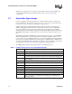
100 0 1
3.4
100 0 0
3.5
111 1 1
no core
Table 2. Core and L2 Voltage Identification Definition
1, 2
(Sheet 2 of 2)
Processor Pins
VID4 VID3 VID2 VID1 VID0 V
CC
Core
3
L2
3