
Datasheet


Pentium
®
III Xeon™ Processor at 500 and 550 MHz
Datasheet
33
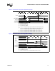
3.1 System Bus Clock Signal Quality Specifications
Table 18 describes the signal quality specifications at the processor core pad for the Pentium
III
Xeon processor system bus clock (BCLK) signal. Figure 13 shows the signal quality waveform for
the system bus clock at the processor core pads. Please see Table 11 for the definition of T numbers
and Table 18 for the definition of V numbers.
NOTES
1. Unless otherwise noted, all specifications in this table apply to all Pentium
®
III Xeon™ processor frequencies
and cache sizes.
2. The rising and falling edge ringback voltage specified is the minimum (rising) or maximum (falling) absolute
voltage the BCLK signal can dip back to after passing the V
IH
(rising) or V
IL
(falling) voltage limits. This
specification is an absolute value.
3.2 AGTL+ Signal Quality Specifications
Many scenarios have been simulated to generate a set of AGTL+ layout guidelines which are
available in the
100 MHz 2-Way SMP Pentium
®
III
Xeon™ Processor/Intel
®
440GX AGPset
AGTL+ Layout Guidelines
and
Pentium
®
III
Xeon™ Processor/Intel
®
450NX PCIset AGTL+
Layout Guidelines
. Also refer to the
Pentium
®
II Processor Developer’s Manual
for the
specification for the GTL+ buffer specification.
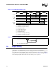
Table 18. BCLK Signal Quality Specifications for Simulation at the Processor Core
1
V# Parameter Min Nom Max Unit Figure Notes
V1: BCLK V
IL
0.7 V 13
V2: BCLK V
IH
1.7 V 13
V3: V
IN
Absolute Voltage Range –0.7 3.3 V 13
V4: Rising Edge Ringback 1.7 V 13 2
V5: Falling Edge Ringback 0.7 V 13 2
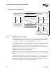
Figure 13. BCLK, TCK, PICCLK Generic Clock Waveform at the Processor Core Pins
V2
V1
V3
V3
T3
V5
V4
T6 T4 T5