
Datasheet


Pentium
®
III Xeon™ Processor at 500 and 550 MHz
Datasheet
49
NOTES
1. Upper address bits are decoded in conjunction with the select pins.
2. A tri-state or “Z” state on this pin is achieved by leaving this pin unconnected.
Note:
System management software must be aware of the slot number-dependent changes in the address
for the thermal sensor.
Though this addressing scheme is targeted for up to 4-way MP systems, more processors can be
supported by using a multiplexed (or separate) SMBus implementation.
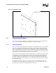
5.0 Thermal Specifications and Design Consideration
The Pentium
III
Xeon processor will use a thermal plate for heatsink attachment. The thermal plate
interface is intended to provide for multiple types of thermal solutions. This chapter will provide
the necessary data for a thermal solution to be developed. See Figure 18 for thermal plate location.
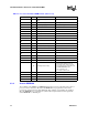
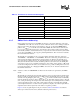
Table 36. Thermal Sensor SMBus Addressing on the Pentium
®
III Xeon™ Processor
Address (Hex) Upper Address
1
Slot Selec 8-bit Address Word on Serial Bus
SA1 SA2 b[7:0]
3Xh 0011 0 0 0011000Xb
0011 1 0 0011010Xb
5Xh 0101 0 Z
2
0101001Xb
0101 1 Z
2
0101011Xb
9Xh 1001 0 1 1001100Xb
1001 1 1 1001110Xb
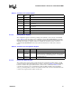
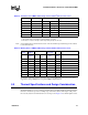
Table 37. Memory Device SMBus Addressing on the Pentium
®
III Xeon™ Processor
Address
(Hex)
Upper
Address
Slot Select
Memory
Device Selec
R/W Device Addressed
bits 7-4
(SA1)
bit 3
(SA0)
bit 2
bit 1 bit 0
A0h/A1h 1010 0 0 0 X Scratch EEPROM 1
A2h/A3h 1010 0 0 1 X Processor Information ROM 1
A4h/A5h 1010 0 1 0 X Scratch EEPROM 2
A6h/A7h 1010 0 1 1 X Processor Information ROM 2
A8h/A9h 1010 1 0 0 X Scratch EEPROM 3
Aah/Abh 1010 1 0 1 X Processor Information ROM 3
Ach/Adh 1010 1 1 0 X Scratch EEPROM 4
Aeh/Afh 1010 1 1 1 X Processor Information ROM 4