Intel® Core™ X-Series Processor Families Datasheet – Volume 1 of 2 Supporting Intel® Core™ X-series Processor Family – i7-7800X, i7-7820X, i9-7900X, i9-7920X, i9-7940X, i9-7960X, i97980XE, i7-9800X, i9-9820X, i9-9900X, i9-9920X, i9-9940X, i99960X, i9-9980XE December 2018 Revision 004 Document Number: 335899-004
® INFORMATION SALE AND/OR UNLESS OTHERWISE USE IN THIS OFAGREED INTEL DOCUMENT PRODUCTS IN WRITING IS PROVIDED INCLUDING BY INTEL, IN CONNECTION LIABILITY THE INTELOR PRODUCTS WITH WARRANTIES IntelARE PRODUCTS.
Contents 1 Introduction ..............................................................................................................7 1.1 Processor Feature Details .....................................................................................8 1.2 Supported Technologies .......................................................................................9 1.3 Interfaces ..........................................................................................................9 1.3.
.3 4.4 4.5 4.6 4.7 4.8 4.9 5 4 Direct Media Interface 3 (DMI3) Signals............................................................... PECI Signal ...................................................................................................... System Reference Clock Signals.......................................................................... JTAG and TAP Signals........................................................................................ Serial VID Interface (SVID) Signals ..........
Figures 1-1 1-2 2-1 2-2 5-1 5-2 5-3 5-4 5-5 5-6 Platform Block Diagram Example ...........................................................................8 PCI Express* Lane Partitioning and Direct Media Interface Generation 3 (DMI3)......... 11 PCI Express* Layering Diagram........................................................................... 18 Packet Flow through the Layers ........................................................................... 18 Input Device Hysteresis........................
Revision History Revision Number Description 001 • Initial release 002 • • • • Updated Updated Updated Updated Section Section Section Section Revision Date May 2017 1.3.1, 1.3.2, 1.4.1, 1.4.2, “System Memory Support” “PCI Express*” “Processor Package and Core States” “System States Support” 003 • Updated Section 1.
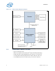
Introduction 1 Introduction The Intel® Core™ X-Series processor families are the next generation of 64-bit, multicore processors built on 14-nm process technology. Based on the low power / high performance processor microarchitecture, the processor is designed for a platform consisting of a processor and Platform Controller Hub (PCH). The X-Series processor is used with the Intel® X299 Chipset PCH. The processor supports up to 46 bits of physical address space and 48 bits of virtual address space.
Introduction Figure 1-1. Platform Block Diagram Example 1.1 Processor Feature Details • Up to 18 execution cores • Each core supports two threads (Intel® Hyper-Threading Technology) • 32 KB instruction and 32 KB data first-level cache (L1) for each core • 1.0 MB private instruction/data mid-level cache (MLC) for each core • 1.
Introduction 1.2 Supported Technologies • Intel® Virtualization Technology (Intel® VT) • Intel® Virtualization Technology (Intel® VT) for Directed I/O (Intel® VT-d) • Intel® Virtualization Technology (Intel® VT) Processor Extensions • Intel® 64 Architecture • Intel® Streaming SIMD Extensions 4.2 (Intel® SSE4.2) • Intel® Advanced Vector Extensions 2.
Introduction 1.3.2 PCI Express* • The PCI Express* port(s) are fully-compliant with the PCI Express* Base Specification, Revision 3.0 (PCIe* 3.0). • Support for PCI Express* 3.0 (8.0 GT/s), 2.0 (5.0 GT/s), and 1.0 (2.5 GT/s). • Up to 44 lanes of PCI Express* interconnect for general purpose PCI Express* devices at PCIe* 3.
Introduction Figure 1-2. PCI Express* Lane Partitioning and Direct Media Interface Generation 3 (DMI3) 1.3.3 Direct Media Interface • Chip-to-chip interface to the PCH. • The DMI3 port supports x4 link width and only operates in a x4 mode when in DMI3. • Operates at PCI Express* 1.0, 2.0, 3.0 speeds. • Transparent to software. • Processor and peer-to-peer writes and reads with 64-bit address support. • APIC and Message Signaled Interrupt (MSI) support.
Introduction 1.3.4 Platform Environment Control Interface (PECI) The PECI is a one-wire interface that provides a communication channel between a PECI client (the processor) and a PECI master (the PCH). • Supports operation at up to two Mbps data transfers. • Link layer improvements to support additional services and higher efficiency over PECI 2.0 generation.
Introduction 1.6 Package Summary The processor socket type is noted as LGA2066. The processor package is a 52.5 x 45 mm FC-LGA package. 1.7 Terminology Table 1-1. Terminology (Sheet 1 of 3) Term Description ASPM Active State Power Management Cbo Caching Agent (also referred to as CA). It is a term used for the internal logic providing ring interface to LLC and Core. The Cbo is a functional unit in the processor. DDR4 Fourth generation Double Data Rate SDRAM memory technology.
Introduction Table 1-1. Terminology (Sheet 2 of 3) Term 14 Description Intel® Turbo Boost Technology A feature that opportunistically enables the processor to run a faster frequency. This results in increased performance of both single and multi-threaded applications.
Introduction Table 1-1. Terminology (Sheet 3 of 3) Term 1.8 Description SMBus System Management Bus. A two-wire interface through which simple system and power management related devices can communicate with the rest of the system. SSE Intel® Streaming SIMD Extensions (Intel® SSE) STD Suspend-to-Disk Storage Conditions A non-operational state. The processor may be installed in a platform, in a tray, or loose. Processors may be sealed in packaging or exposed to free air.
Introduction Table 1-2. Related Documents (Sheet 2 of 2) Document Number/ Location Document PCI Express* Base Specification, Revision 3.0 PCI Express* Base Specification, Revision 2.1 http://www.pcisig.com/ PCI Express* Base Specification, Revision 1.1 PCIe* Gen 3 Connector High Speed Electrical Test Procedure 325028-001 / http://www.intel.com/ content/www/us/en/io/pciexpress/pci-expressarchitecture-devnetresources.html Connector Model Quality Assessment Methodology 326123-002 / http://www.intel.
Interfaces 2 Interfaces This chapter describes the functional behaviors supported by the processor. Topics covered include: • System Memory Interface • PCI Express* Interface • Direct Media Interface 3 (DMI3) / PCI Express* Interface • Platform Environment Control Interface (PECI) 2.1 System Memory Interface 2.1.1 System Memory Technology Support The Integrated Memory Controller (IMC) supports DDR4 protocols with four independent 64-bit memory channels and supports one unbuffered DIMM per channel. 2.
Interfaces Figure 2-1. PCI Express* Layering Diagram PCI Express* uses packets to communicate information between components. Packets are formed in the Transaction and Data Link Layers to carry the information from the transmitting component to the receiving component. As the transmitted packets flow through the other layers, the packets are extended with additional information necessary to handle packets at those layers.
Interfaces The transmission side of the Data Link Layer accepts TLPs assembled by the Transaction Layer, calculates and applies data protection code and TLP sequence number, and submits them to Physical Layer for transmission across the Link. The receiving Data Link Layer is responsible for checking the integrity of received TLPs and for submitting them to the Transaction Layer for further processing.
Interfaces 2.3.2 Processor / PCH Compatibility Assumptions The processor is compatible with the PCH and is not compatible with any previous Intel® Memory Controller Hub (MCH) and Integrated Controller Hub (ICH) products. 2.3.3 DMI3 Link Down The DMI3 link going down is a fatal, unrecoverable error. If the DMI3 data link goes to data link down, after the link was up, then the DMI3 link hangs the system by not allowing the link to retrain to prevent data corruption. This is controlled by the PCH.
Technologies 3 Technologies This chapter covers the following technologies: • Intel® Virtualization Technology (Intel® VT) • Security Technologies • Intel® Hyper-Threading Technology (Intel® HT Technology) • Intel® Turbo Boost Technology • Enhanced Intel SpeedStep® Technology • Intel® Advanced Vector Extensions (Intel® AVX) 3.1 Intel® Virtualization Technology (Intel® VT) Intel® Virtualization Technology (Intel® VT) makes a single system appear as multiple independent systems to software.
Technologies 3.1.2 Intel® VT-x Features The processor core supports the following Intel® VT-x features: • Extended Page Tables (EPT) — hardware assisted page table virtualization. — eliminates VM exits from guest operating system to the VMM for shadow pagetable maintenance. • Virtual Processor IDs (VPID) — Ability to assign a VM ID to tag processor core hardware structures (such as, TLBs).
Technologies 3.1.3.
Technologies 3.2 Security Technologies 3.2.1 Intel® Advanced Encryption Standard New Instructions (Intel® AES-NI) Instructions These instructions enable fast and secure data encryption and decryption, using the Advanced Encryption Standard (Intel® AES-NI) which is defined by FIPS Publication number 197. Since Intel® AES-NI is the dominant block cipher, and it is deployed in various protocols, the new instructions will be valuable for a wide range of applications.
Technologies 3.4 Intel® Turbo Boost Max Technology 3.0 Intel® Turbo Boost Technology is a feature that allows the processor to opportunistically and automatically run faster than its rated operating frequency if it is operating below power, temperature, and current limits. The result is increased performance in multi-threaded and single threaded workloads. It should be enabled in the BIOS for the processor to operate with maximum performance. Processors with Intel® Turbo Boost Max Technology 3.
Technologies allows logic to remain active. The core clock can also restart more quickly under Enhanced Intel SpeedStep Technology. 3.6 Intel® Advanced Vector Extensions (Intel® AVX) Intel® Advanced Vector Extensions (Intel® AVX) is a new 256-bit vector SIMD extension of Intel Architecture. The introduction of Intel AVX started with the Second Generation Intel® Core™ processor family.
Technologies • Additional computational and/or data manipulation primitives • Compatibility – Intel® AVX is backward compatible with previous ISA extensions including Intel® SSE4: — Existing Intel® SSE applications/library can: • Run unmodified and benefit from processor enhancements • Recompile existing Intel® SSE intrinsic using compilers that generate Intel® AVX code • Inter-operate with library ported to Intel® AVX — Applications compiled with Intel® AVX can inter-operate with existing Intel® SSE libra
Signal Descriptions 4 Signal Descriptions This chapter describes the signals. They are arranged in functional groups according to their associated interface or category. 4.1 System Memory Interface Table 4-1. Memory Channel DDR0, DDR1, DDR2, DDR3, DDR4, DDR5 Signal Name DDR{5:0}_ACT_N Description Activate. When asserted, indicates MA[16:14] are command signals (RAS_N, CAS_N, WE_N). DDR{5:0}_ALERT_N Parity Error detected by the DIMM (one for each channel). DDR{5:0}_BA[1:0] Bank Address.
Signal Descriptions Table 4-2. Memory Channel Miscellaneous Signal Name Description DDR {012,345}_RESET_N System memory reset: Reset signal from processor to DRAM devices on the DIMMs. DDR012_RESET_N is used for memory channels 0, 1 and 2 while DDR345_RESET_N is used for memory channels 3, 4 and 5. DDR{012,345}_SPDSCL SMBus clock for the dedicated interface to the serial presence detect (SPD) and thermal sensors (TSoD) on the DIMMs.
Signal Descriptions 4.4 PECI Signal Table 4-6. PECI Signal Signal Name Description PECI (Platform Environment Control Interface) is the serial sideband interface to the processor and is used primarily for thermal, power and error management. PECI 4.5 System Reference Clock Signals Table 4-7. System Reference Clock (BCLK{0/1/2}) Signals Signal Name BCLK{0,1,2}_DN/DP Description Reference Clock Differential input.
Signal Descriptions 4.7 Serial VID Interface (SVID) Signals Table 4-9. SVID Signals Signal Name 4.8 Description SVIDALERT_N [1:0] Serial VID alert. SVIDCLK [1:0] Serial VID clock. SVIDDATA [1:0] Serial VID data out. Processor Asynchronous Sideband and Miscellaneous Signals Table 4-10. Processor Asynchronous Sideband Signals (Sheet 1 of 2) Signal Name Description CATERR_N Indicates that the system has experienced a fatal or catastrophic error and cannot continue to operate.
Signal Descriptions Table 4-10. Processor Asynchronous Sideband Signals (Sheet 2 of 2) Signal Name Description PWRGOOD PWRGOOD is a processor input. The processor requires this signal to be a clean indication that all processor clocks and power supplies are stable and within their specifications. “Clean” implies that the signal will remain low (capable of sinking leakage current), without glitches, from the time that the power supplies are turned on until they come within specification.
Signal Descriptions Table 4-11. Miscellaneous Signals (Sheet 2 of 3) Signal Name Description EAR_N External Alignment of Reset, used to bring the processor up into a deterministic state. This signal is pulled up on the die, refer to Table 5-7, “Signals with On-Die Weak PU/PD” for details. FIVR_FAULT Indicates an internal error has occurred with the integrated voltage regulator. The FIVR_FAULT signal can be sampled any time after 1.5 ms after the assertion of PWRGOOD.
Signal Descriptions Table 4-11. Miscellaneous Signals (Sheet 3 of 3) Signal Name TXT_PLTEN 4.9 Description Intel® Trusted Execution Technology (Intel® TXT) Platform Enable Strap. 0 = The platform is not Intel® TXT enabled. All sockets should be set to zero. Scalable DP (sDP) platforms should choose this setting if the Node Controller does not support Intel® TXT. 1 = Default. The platform is Intel® TXT enabled. All sockets should be set to one. In a non-Scalable DP platform this is the default.
Electrical Specifications 5 Electrical Specifications This chapter describes processor signaling and DC specifications. References to various interfaces (memory, PCIe* PECI, and so forth) are also described. 5.1 Integrated Voltage Regulation The platform voltage regulator is integrated into the processor. Due to this integration, the processor has one main voltage rail (VCCIN) and a voltage rail for the memory interface (VCCD012, VCCD345 - one for each memory channel pair).
Electrical Specifications 5.2.4 Platform Environmental Control Interface (PECI) PECI is an Intel proprietary interface that provides a communication channel between Intel processors and chipset components to external system management logic and thermal monitoring devices. The processor contains a Digital Thermal Sensor (DTS) that reports a relative die temperature as an offset from Thermal Control Circuit (TCC) activation temperature.
Electrical Specifications Clock multiplying within the processor is provided by the internal phase locked loop (PLL), which requires a constant frequency BCLK{0/1/2}_DP, BCLK{0/1/2}_DN input, with exceptions for spread spectrum clocking. DC specifications for the BCLK{0/1/ 2}_DP, BCLK{0/1/2}_DN inputs are provided in Section 5.5.2.7. 5.2.
Electrical Specifications 5.2.8.2 Decoupling Guidelines Due to its large number of transistors and high internal clock speeds, the processor is capable of generating large current swings between low and full power states. This may cause voltages on power planes to sag below their minimum values if bulk decoupling is not adequate. Large electrolytic bulk capacitors (CBULK), help maintain the output voltage during current transients, for example coming out of an idle condition.
Electrical Specifications Power source characteristics must be guaranteed to be stable whenever the supply to the voltage regulator is stable. 5.2.8.5 SetWP Working Point Command The SetWP is a command that invokes a look up table for VID set points. During the initial power on phase the CPU will program the WPx registers (WP0=3Ah..WP7=41h) on a per rail address basis.
Electrical Specifications The SetVID_Fast command is preemptive. The VR interrupts its current processes and moves to the new VID. The SetVID_Fast command operates on 1 VR address at a time. This command is used in the processor for package C6 fast exit. 5.2.8.7 SetVID Slow The SetVID_Slow command contains the target VID in the payload byte. The range of voltage is defined in the VID table. The VR should ramp to the new VID setting with a “slow” slew rate as defined in the slow slew rate data register.
Electrical Specifications Table 5-3. SVID Address Usage Bus 2 PWM Address (HEX) 00 Protocol ID 04H(10mV VID) or 07H(5mV VID) 01 Processor VCCD012 NA 02 04H(10mV VID) or 07H(5mV VID) 03 VCCD345 NA Notes: 1. Check with VR vendors for determining the physical address assignment method for their controllers. 2. VR addressing is assigned on a per voltage rail basis. 3. Dual VR controllers will have two addresses with the lowest order address, always being the higher phase count. Table 5-4. VR13.
Electrical Specifications Table 5-4. VR13.0 Reference Code Voltage Identification (VID) Table (Sheet 2 of 2) HEX VCCIN HEX VCCIN HEX VCCIN HEX VCCIN HEX VCCIN 1E 0.79 3E 1.11 5E 1.43 7E 1.75 9E 1F 0.80 3F 1.12 5F 1.44 7F 1.76 9F HEX VCCIN HEX VCCIN HEX VCCIN 2.07 BE 2.39 DE 2.71 FE 3.03 2.08 BF 2.40 DF 2.72 FF 3.04 Notes: 1. 00h = Off State 2. VID Range HEX 65-97 are not used by the processor 3. VCCD can use Protocol ID of 10 mV or 5 mV. 4.
Electrical Specifications Table 5-6.
Electrical Specifications Table 5-6. Signal Groups (Sheet 2 of 2) Differential/Single Ended Buffer Type Signal System Reference Clock (BCLK{0/1/2}) Differential CMOS 1.
Electrical Specifications Table 5-7. Signals with On-Die Weak PU/PD Signal Name BIST_ENABLE 5.3.
Electrical Specifications Table 5-8. Power-On Configuration Option Lands (Sheet 2 of 2) Configuration Option Land Name Notes Enable Intel® Trusted Execution Technology (Intel® TXT) Agent TXT_AGENT Enable Safe Mode Boot SAFE_MODE_BOOT 3 Configure Socket ID SOCKET_ID[1:0] 3 Enable legacy socket boot LEGACY_SKT 3 3 Notes: 1. Output tri-state option enables Fault Resilient Booting (FRB), for FRB details, refer to the Fault Resilient Booting (FRB) Section.
Electrical Specifications maximum or minimum device storage conditions for a sustained period of time. At conditions outside sustained limits, but within absolute maximum and minimum ratings, quality and reliability may be affected. Table 5-10. Storage Condition Ratings Symbol Tabsolute storage Parameter The minimum/maximum device storage temperature beyond which damage (latent or otherwise) may occur when subjected to for any length of time.
Electrical Specifications Table 5-11. Voltage Specification (Sheet 2 of 2) Symbols Parameter V CCD (V CCD_012, V CCD_345) I/O Voltage for DDR4 (Standard Voltage) VCCSA Power supply for IIO VCCIO IO voltage supply input VCC33 Power supply for PIROM Voltage Plane Min Nom Max Unit VCCD 1.17 1.2 1.26 V 0.5 — 1.1 V — 0.937 1.00 1.057 V 3.14 3.3 3.47 V Notes1 7, 9, 10, 11 Notes: 1. Unless otherwise noted, all specifications in this table apply to all processors. 2.
Electrical Specifications Table 5-12. Current (ICCIN_MAX and ICCIN_TDC) Specification (Sheet 2 of 2) TDP (W) 140 Pmax VCCIN (W) Pmax Package (W) 297 Notes: 1. Unless otherwise noted, all specifications in this table apply to all processors. 2. N/A 3. ICCIN_TDC (Thermal Design Current) is the sustained (DC equivalent) current that the processor is capable of drawing indefinitely and should be used for the voltage regulator thermal assessment.
Electrical Specifications Table 5-13. VCCIN Static and Transient Tolerance for 1.0LL (Sheet 2 of 2) ICCIN (A) VCCIN_Max (V) VCCIN_Nom (V) VCCIN_Min (V) 220 VID -0.198 VID -0.220 VID -0.242 230 VID - 0.208 VID - 0.230 VID - 0.252 Notes Notes: 1. The VCCIN_MIN and VCCIN_MAX loadlines represent static and transient limits. 2. This table is intended to aid in reading discrete points on graph in Figure 5-2, “VCCIN Static and Transient Tolerance Load Lines 1.0 mOHM” on page 50. 3.
Electrical Specifications Symbol Parameter Min Nom Max Units — (V CCD / 2)* (R ON / (R ON +R VTT_TERM )) — V - ((V CCD / 2)* (R ON /(R ON +R VTT_TERM ))) — V — Vol=(Ron / (Ron + RVDD_TERM)) *VCCD — V — VCCD — V DDR4 Clock Buffer On Resistance 25.5 30 34.
Electrical Specifications 5.5.2.2 Symbol PECI DC Specifications Definition and Conditions Min Max Units -0.15 0.15 + VCCIO V Figure Notes1 VIn Input Voltage Range VHysteresis Hysteresis 0.1*VCCIO — V VN Negative-edge threshold voltage 0.275*VCCIO 0.500*VCCIO V Figure 5-1 2 VP Positive-edge threshold voltage 0.550*VCCIO 0.725*VCCIO V Figure 5-1 2 I Pullup Resistance (VOH = 0.75*VCCIO) -6.
Electrical Specifications Symbol Parameter Signal Min Max Unit Figure Notes1 IIL Input Leakage Current N/A — 1.50 mA 8, 9 Cpad Pad Capacitance N/A 1.90 1.72 pF 9 Notes: 1. Unless otherwise noted, all specifications in this table apply to all processor frequencies. 2. Crossing Voltage is defined as the instantaneous voltage value when the rising edge of BCLK{0/1}_DN is equal to the falling edge of BCLK{0/1}_DP. 3. VHavg is the statistical average of the VH measured by the oscilloscope.
Electrical Specifications Figure 5-5. BCLK{0/1/2} Single Ended Clock Measurement Points for Absolute Cross Point and Swing Figure 5-6. BCLK{0/1/2} Single Ended Clock Measure Points for Delta Cross Point 5.5.2.4 SMBus DC Specifications Symbol Parameter Min Max Units — 0.3*VCCIO V Input High Voltage 0.7*VCCIO — V Hysteresis 0.1*VCCIO — V Output Low Voltage — 0.
Electrical Specifications Symbol Parameter Min Max Units IIL Input Leakage Current Signals ±50 ±200 μA SR Output Edge Rate (50 ohm to VCCIO) Signal: BPM_N[7:0], PRDY_N, TDO 1.13 5 V/ns Notes 1 Notes: 1. These are measured between VIL and VIH. 2. The signal edge rate must be met or the signal must transition monotonically to the asserted state. 5.5.2.6 Serial VID Interface (SVID) DC Specifications Symbol Parameter Min Nom Max Units VCCIO - 5% 1.
Electrical Specifications Symbol Parameter RON Buffer On Resistance SR Output Edge Rate Min Max Units Notes 1, 2, 4 14 4 1.13 5 V/ns 3, 5 Notes: 1. This table applies to the processor sideband and miscellaneous signals specified in Table 5-6, “Signal Groups”. 2. Unless otherwise noted, all specifications in this table apply to all processor frequencies. 3. These are measured between VIL and VIH. 4.