
Datasheet


Intel
®
Core
TM
i7-660UE, i7-620LE/UE, i7-610E, i5-520E, i3-330E and Intel
®
Celeron
®
Processor P4505, U3405 Series
August 2010 Datasheet Addendum
Document Number: 323178-003 103
Processor Configuration Registers
6.2.23 INTRPIN6 - Interrupt Pin
B/D/F/Type: 0/6/0/PCI
Address Offset: 3Dh
Default Value: 01h
Access: RO
Size: 8 bits
This register specifies which interrupt pin this device uses.
6.2.24 BCTRL6 - Bridge Control
B/D/F/Type: 0/6/0/PCI
Address Offset: 3E-3Fh
Default Value: 0000h
Access: RO; RW
Size: 16 bits
This register provides extensions to the PCICMD6 register that are specific to PCI-PCI
bridges. The BCTRL provides additional control for the secondary interface (i.e., PCI
Express-G) as well as some bits that affect the overall behavior of the “virtual” Host-
PCI Express bridge embedded within processor, e.g., VGA compatible address ranges
mapping.
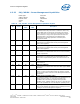
Table 46. INTRPIN6 - Interrupt Pin Register
Bit Access
Default
Value
RST/
PWR
Description
7:0 RO 01h Core Interrupt Pin (INTPIN)
As a single function device, the PCI Express device specifies INTA
as its interrupt pin. 01h=INTA.
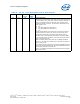
Table 47. BCTRL6 - Bridge Control Register (Sheet 1 of 2)
Bit Access
Default
Value
RST/
PWR
Description
15:12 RO 0h Core Reserved
11 RO 0b Core Discard Timer SERR# Enable (DTSERRE)
Not Applicable or Implemented. Hard wired to 0.
10 RO 0b Core Discard Timer Status (DTSTS)
Not Applicable or Implemented. Hard wired to 0.
9RO 0bCoreSecondary Discard Timer (SDT)
Not Applicable or Implemented. Hard wired to 0.
8RO 0bCorePrimary Discard Timer (PDT)
Not Applicable or Implemented. Hard wired to 0.
7RO 0bCoreFast Back-to-Back Enable (FB2BEN)
Not Applicable or Implemented. Hard wired to 0.
6RW 0bCoreSecondary Bus Reset (SRESET)
Setting this bit triggers a hot reset on the corresponding PCI
Express Port. This will force the LTSSM to transition to the Hot
Reset state (via Recovery) from L0, L0s, or L1 states.