
Datasheet


Intel
®
Core
TM
i7-660UE, i7-620LE/UE, i7-610E, i5-520E, i3-330E and Intel
®
Celeron
®
Processor P4505, U3405 Series
August 2010 Datasheet Addendum
Document Number: 323178-003 111
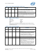
Processor Configuration Registers
6.2.31 MA - Message Address
B/D/F/Type: 0/6/0/PCI
Address Offset: 94-97h
Default Value: 00000000h
Access: RO; RW
Size: 32 bits
6.2.32 MD - Message Data
B/D/F/Type: 0/6/0/PCI
Address Offset: 98-99h
Default Value: 0000h
Access: RW
Size: 16 bits
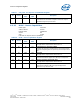
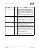
Table 54. MA - Message Address Register
Bit Access
Default
Value
RST/
PWR
Description
31:2 RW 00000000h Core Message Address (MA)
Used by system software to assign an MSI address to the
device. The device handles an MSI by writing the padded
contents of the MD register to this address.
1:0 RO 00b Core Force DWord Align (FDWA)
hard wired to 0 so that addresses assigned by system software
are always aligned on a dword address boundary.
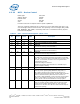
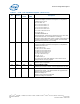
Table 55. MD - Message Data Register
Bit Access
Default
Value
RST/
PWR
Description
15:0 RW 0000h Core Message Data (MD)
Base message data pattern assigned by system software and
used to handle an MSI from the device.
When the device must generate an interrupt request, it writes a
32-bit value to the memory address specified in the MA register.
The upper 16 bits are always set to 0. The lower 16 bits are
supplied by this register.