
Datasheet

Intel
®
Core
TM
i7-660UE, i7-620LE/UE, i7-610E, i5-520E, i3-330E and Intel
®
Celeron
®
Processor P4505, U3405 Series
August 2010 Datasheet Addendum
Document Number: 323178-003 25
Electrical Specifications
4 Electrical Specifications
4.1 Signal Groups
Signals are grouped by buffer type and similar characteristics as listed in Table 10. The
buffer type indicates which signaling technology and specifications apply to the signals.
All the differential signals, and selected DDR3 and Control Sideband signals have On-
Die Termination (ODT) resistors. There are some signals that do not have ODT and
need to be terminated on the board.
All Control Sideband Asynchronous signals are required to be asserted/deasserted for
at least eight BCLKs in order for the processor to recognize the proper signal state. See
Section 4.2 for the DC specifications.
4.2 DC Specifications
The processor DC specifications in this section are defined at the processor
pins, unless noted otherwise. See Chapter 5 for the processor pin listings and
Chapter 3 for signal definitions.
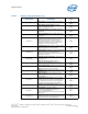
The DC specifications for the DDR3 signals are listed in Table 11.
4.2.1 Voltage and Current Specifications
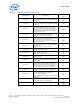
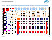
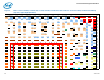
Table 10. Mobile Signal Groups
1
Signal Group
Alpha
Group
Type Signals
DDR3 Data Signals
2
Single ended (e) DDR3 Bi-directional SA_DQ[71:0], SB_DQ[71:0]
Differential (f) DDR3 Bi-directional
SA_DQS[8:0], SA_DQS#[8:0]
SB_DQS[8:0], SB_DQS#[8:0]
Power/Ground/Other
Single Ended (z) Other DBR#, PROC_DETECT, VCAP0, VCAP1, VCAP2
NOTES:
1. Refer to Chapter 3 for signal description details.
2. SA and SB refer to DDR3 Channel A and DDR3 Channel B.
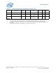
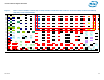
Table 11. DDR3 Signal Group DC Specifications (Sheet 1 of 2)
Symbol Parameter
Alpha
Group
Min Typ Max Units Notes
1,9
V
IL
Input Low Voltage (e,f) 0.43*V
DDQ
V2,4
NOTES:
1. Unless otherwise noted, all specifications in this table apply to all processor frequencies.
2. V
IL
is defined as the maximum voltage level at a receiving agent that will be interpreted as a logical low value.
3. V
IH
is defined as the minimum voltage level at a receiving agent that will be interpreted as a logical high value.
4. V
IH
and V
OH
may experience excursions above V
DDQ
. However, input signal drivers must comply with the signal quality
specifications.
5. R
VTT_TERM
is the termination on the DIMM and in not controlled by the processor.