
Datasheet


Intel
®
Core
TM
i7-660UE, i7-620LE/UE, i7-610E, i5-520E, i3-330E and Intel
®
Celeron
®
Processor P4505, U3405 Series
August 2010 Datasheet Addendum
Document Number: 323178-003 3
Contents
1 Introduction and Features Summary .........................................................................8
1.1 Introduction .......................................................................................................8
1.2 Interfaces ........................................................................................................10
1.2.1 System Memory Support.........................................................................10
1.2.2 PCI Express* .........................................................................................10
1.3 Package...........................................................................................................11
1.4 Terminology .....................................................................................................12
1.5 Related Documents ...........................................................................................13
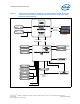
2Interfaces................................................................................................................15
2.1 System Memory Interface ..................................................................................15
2.1.1 System Memory Technology Supported.....................................................15
2.1.2 System Memory Timing Support...............................................................16
2.1.3 System Memory Organization Modes.........................................................16
2.1.4 Rules for Populating Memory Slots............................................................18
2.1.5 Technology Enhancements of Intel
®
Fast Memory Access (Intel
®
FMA)..........18
2.1.6 DRAM Clock Generation...........................................................................19
2.1.7 DDR3 On-Die Termination .......................................................................19
2.2 PCI Express* Interface.......................................................................................19
2.2.1 PCI Express* Configuration Mechanism .....................................................19
2.2.2 PCI Express Port Bifurcation.....................................................................20
3 Signal Description ...................................................................................................21
3.1 System Memory Interface ..................................................................................21
3.2 Reset and Miscellaneous Signals..........................................................................24
4 Electrical Specifications...........................................................................................25
4.1 Signal Groups...................................................................................................25
4.2 DC Specifications ..............................................................................................25
4.2.1 Voltage and Current Specifications............................................................25
5 Processor Ball and Signal Information.....................................................................27
5.1 Processor Ball Assignments.................................................................................27
6 Processor Configuration Registers...........................................................................70
6.1 Register Terminology.........................................................................................70
6.1.1 DEVEN - Device Enable ...........................................................................72
6.1.2 ERRSTS - Error Status ............................................................................73
6.1.3 ERRCMD - Error Command ......................................................................74
6.1.4 SMICMD - SMI Command........................................................................76
6.1.5 C0WRDATACTRL - Channel 0 Write Data Control.........................................77
6.1.6 COECCERRLOG - Channel 0 ECC Error Log.................................................78
6.1.7 C1WRDATACTRL - Channel 1 Write Data Control.........................................80
6.1.8 C1ECCERRLOG - Channel 1 ECC Error Log .................................................80
6.2 PCI Device 6.....................................................................................................81
6.2.1 VID6 - Vendor Identification ....................................................................85
6.2.2 DID6 - Device Identification.....................................................................85
6.2.3 PCICMD6 - PCI Command........................................................................86
6.2.4 PCISTS6 - PCI Status..............................................................................88
6.2.5 RID6 - Revision Identification...................................................................90
6.2.6 CC6 - Class Code ...................................................................................90
6.2.7 CL6 - Cache Line Size .............................................................................91
6.2.8 HDR6 - Header Type...............................................................................91
6.2.9 PBUSN6 - Primary Bus Number ................................................................92