
Datasheet

Processor Configuration Registers
Intel
®
Core
TM
i7-660UE, i7-620LE/UE, i7-610E, i5-520E, i3-330E and Intel
®
Celeron
®
Processor P4505, U3405 Series
Datasheet Addendum August 2010
82 Document Number: 323178-003
Reserved and Preserved:
1. Reserved for future RW implementations; software must preserve value read for
writes to bits.
2. Reserved and Zero: Reserved for future R/WC/S implementations; software must
use 0 for writes to bits.
Unless explicitly documented as Reserved and Zero, all bits marked as reserved are
part of the Reserved and Preserved type, which have historically been the typical
definition for Reserved.
It is important to note that most (if not all) control bits in this device cannot be
modified unless the link is down. Software is required to first Disable the link, then
program the registers, and then re-enable the link (which will cause a full-retrain with
the new settings).
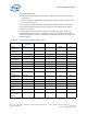
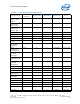
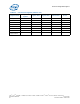
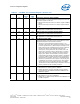
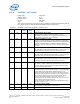
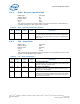
Table 23. PCI Device 6 Register (Sheet 1 of 3)
Register Name
Register
Symbol
Register Start Register End Default Value Access
Vendor
Identification
VID6 0 1 8086h RO
Device
Identification
DID6 2 3 0047h RO
PCI Command PCICMD6 4 5 0000h RO; RW
PCI Status PCISTS6 6 7 0010h RO; RWC
Revision
Identification
RID6 8 8 10h RO
Class Code CC6 9 B 060400h RO
Cache Line Size CL6 C C 00h RW
Header Type HDR6 E E 01h RO
Primary Bus
Number
PBUSN6 18 18 00h RO
Secondary Bus
Number
SBUSN6 19 19 00h RW
Subordinate Bus
Number
SUBUSN6 1A 1A 00h RW
I/O Base Address IOBASE6 1C 1C F0h RO; RW
I/O Limit Address IOLIMIT6 1D 1D 00h RO; RW
Secondary Status SSTS6 1E 1F 0000h RWC; RO
Memory Base
Address
MBASE6 20 21 FFF0h RO; RW
Memory Limit
Address
MLIMIT6 22 23 0000h RO; RW
Prefetchable
Memory Base
Address
PMBASE6 24 25 FFF1h RO; RW