
Datasheet


Processor Configuration Registers
Intel
®
Core
TM
i7-660UE, i7-620LE/UE, i7-610E, i5-520E, i3-330E and Intel
®
Celeron
®
Processor P4505, U3405 Series
Datasheet Addendum August 2010
98 Document Number: 323178-003
6.2.17 PMBASE6 - Prefetchable Memory Base Address
B/D/F/Type: 0/6/0/PCI
Address Offset: 24-25h
Default Value: FFF1h
Access: RO; RW
Size: 16 bits
This register in conjunction with the corresponding Upper Base Address register
controls the CPU to PCI Express-G prefetchable memory access routing based on the
following formula:
PREFETCHABLE_MEMORY_BASE =< address =< PREFETCHABLE_MEMORY_LIMIT
The upper 12 bits of this register are read/write and correspond to address bits
A[31:20] of the 40-bit address. The lower 8 bits of the Upper Base Address register are
read/write and correspond to address bits A[39:32] of the 40-bit address. This register
must be initialized by the configuration software. For the purpose of address decode
address bits A[19:0] are assumed to be 0. Thus, the bottom of the defined memory
address range is aligned to a 1-MB boundary.
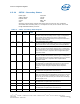
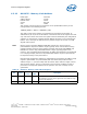
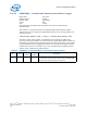
Table 40. PMBASE6 - Prefetchable Memory Base Address Register
Bit Access
Default
Value
RST/
PWR
Description
15:4 RW FFFh Core Prefetchable Memory Base Address (MBASE)
Corresponds to A[31:20] of the lower limit of the memory range
that is passed to PCI Express-G.
3:0 RO 1h Core 64-bit Address Support (64-bit Address Support)
Indicates that the upper 32 bits of the prefetchable memory
region base address are contained in the Prefetchable Memory
base Upper Address register at 28h.