
Intel Celeron D Processor 300 Sequence

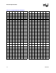
Table Of Contents
- Contents
- Revision History
- 1 Introduction
- 2 Electrical Specifications
- 2.1 FSB and GTLREF
- 2.2 Power and Ground Lands
- 2.3 Decoupling Guidelines
- 2.4 Voltage Identification
- 2.5 Reserved, Unused, and TESTHI Signals
- 2.6 FSB Signal Groups
- 2.7 GTL+ Asynchronous Signals
- 2.8 Test Access Port (TAP) Connection
- 2.9 FSB Frequency Select Signals (BSEL[2:0])
- 2.10 Absolute Maximum and Minimum Ratings
- 2.11 Processor DC Specifications
- 2.12 VCC Overshoot Specification
- 2.13 GTL+ FSB Specifications
- 3 Package Mechanical Specifications
- 4 Land Listing and Signal Descriptions
- 5 Thermal Specifications and Design Considerations
- 6 Features
- 7 Boxed Processor Specifications
- 8 Debug Tools Specifications
16 Datasheet
Electrical Specifications
2.3.1 V
CC
Decoupling
Regulator solutions need to provide bulk capacitance with a low Effective Series Resistance (ESR)
and keep a low interconnect resistance from the regulator to the socket. Bulk decoupling for the
large current swings when the part is powering on, or entering/exiting low power states, must be
provided by the voltage regulator solution (VR). For more details, refer to the Voltage Regulator
Down (VRD) 10.1 Design Guide For Desktop LGA775 Socket.
2.3.2 FSB GTL+ Decoupling
The Celeron D processor in the 775-land package integrates signal termination on the die as well as
incorporating high frequency decoupling capacitance on the processor package. Decoupling must
also be provided by the system baseboard for proper GTL+ bus operation.
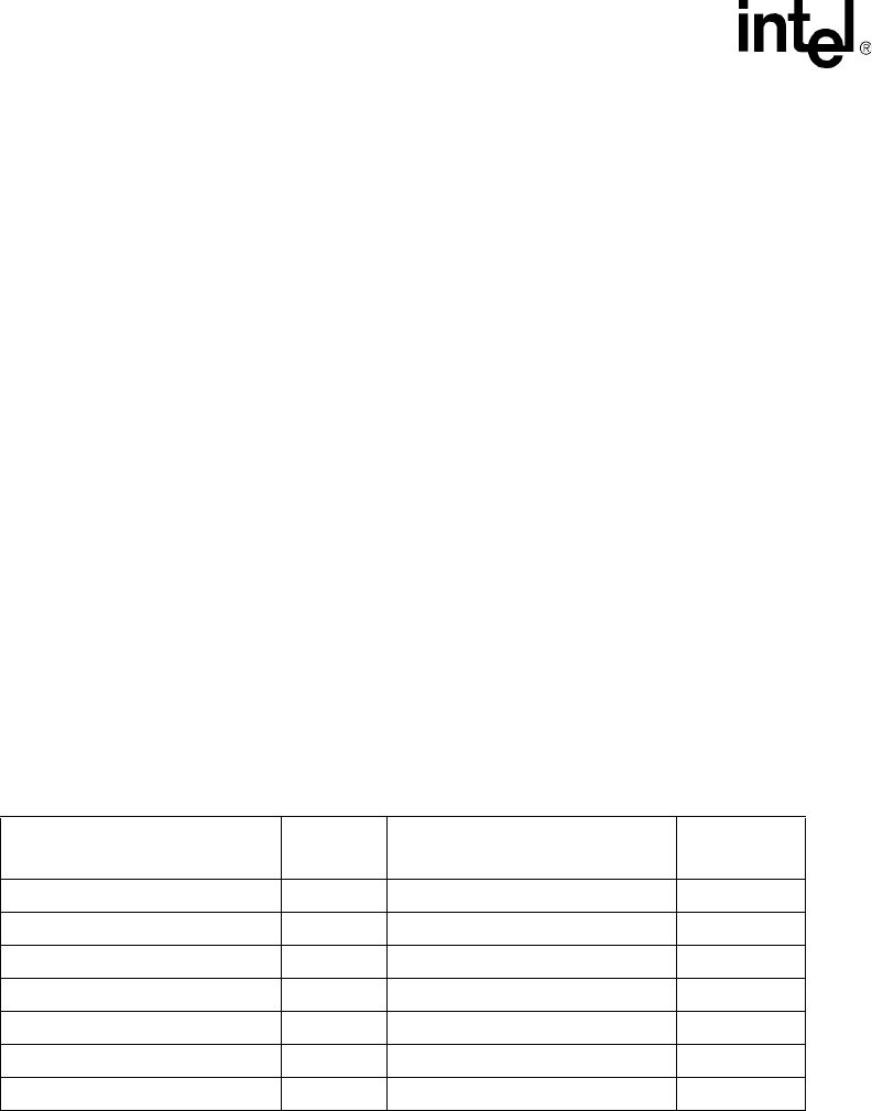
2.3.3 FSB Clock (BCLK[1:0]) and Processor Clocking
BCLK[1:0] directly controls the FSB interface speed as well as the core frequency of the processor.
As in previous generation processors, the Celeron D processor in the 775-land package core
frequency is a multiple of the BCLK[1:0] frequency. Refer to Table 2-1 for the Celeron D
processor in the 775-land package supported ratios.
The Celeron D processor in the 775-land package uses a differential clocking implementation. For
more information on the Celeron D processor in the 775-land package clocking, refer to the
CK410/CK410M Clock Synthesizer/Driver Specification.
Table 2-1. Core Frequency to FSB Multiplier Configuration
Multiplication of System Core
Frequency to FSB Frequency
Processor
Number
Core Frequency (133 MHz BCLK
/ 533 MHz FSB)
Notes
1
NOTES:
1. Individual processors operate only at or below the rated frequency.
1/19 325J/326 2.53 GHz —
1/20 330J/331 2.66 GHz —
1/21 335J/336 2.80 GHz —
1/22 340J/341 2.93 GHz —
1/23 345J/346 3.06 GHz —
1/24 351 3.20 GHz —
1/25 355 3.33 GHz —