
Intel Celeron D Processor 300 Sequence
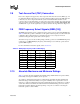
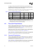
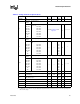
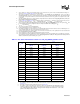
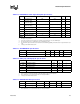
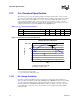
Table Of Contents
- Contents
- Revision History
- 1 Introduction
- 2 Electrical Specifications
- 2.1 FSB and GTLREF
- 2.2 Power and Ground Lands
- 2.3 Decoupling Guidelines
- 2.4 Voltage Identification
- 2.5 Reserved, Unused, and TESTHI Signals
- 2.6 FSB Signal Groups
- 2.7 GTL+ Asynchronous Signals
- 2.8 Test Access Port (TAP) Connection
- 2.9 FSB Frequency Select Signals (BSEL[2:0])
- 2.10 Absolute Maximum and Minimum Ratings
- 2.11 Processor DC Specifications
- 2.12 VCC Overshoot Specification
- 2.13 GTL+ FSB Specifications
- 3 Package Mechanical Specifications
- 4 Land Listing and Signal Descriptions
- 5 Thermal Specifications and Design Considerations
- 6 Features
- 7 Boxed Processor Specifications
- 8 Debug Tools Specifications
22 Datasheet
Electrical Specifications
.
2.7 GTL+ Asynchronous Signals
Legacy input signals such as A20M#, IGNNE#, INIT#, SMI#, and STPCLK# use CMOS input
buffers. All of these signals follow the same DC requirements as GTL+ signals; however, the
outputs are not actively driven high (during a logical 0 to 1 transition) by the processor. These
signals do not have setup or hold time specifications in relation to BCLK[1:0].
All of the GTL+ Asynchronous signals are required to be asserted/de-asserted for at least six
BCLKs for the processor to recognize the proper signal state. See Section 2.11 for the DC
specifications for the GTL+ Asynchronous signal groups. See Section 6.2 for additional timing
requirements for entering and leaving the low power states.
Table 2-4. Signal Characteristics
Signals with R
TT
Signals with no R
TT
A[35:3]#, ADS#, ADSTB[1:0]#, AP[1:0]#, BINIT#,
BNR#, BOOTSELECT
1
, BPRI#, D[63:0]#, DBI[3:0]#,
DBSY#, DEFER#, DP[3:0]#, DRDY#, DSTBN[3:0]#,
DSTBP[3:0]#, HIT#, HITM#, LOCK#, MCERR#,
PROCHOT#, REQ[4:0]#, RS[2:0]#, RSP#, TRDY#,
EDRDY#
2
, PC_REQ#
2
NOTES:
1. The BOOTSELECT signal has a 500–5000 Ω pull-up to V
TT
rather than on-die termination.
2. EDRDY# and PC_REQ# are not features of the Celeron D processor in the 775-land package. They are included here for
future processor compatibility.
A20M#, BCLK[1:0], BPM[5:0]#, BR0#, BSEL[2:0],
COMP[5:0], FERR#/PBE#, IERR#, IGNNE#,
INIT#, LINT0/INTR, LINT1/NMI, PWRGOOD,
RESET#, SKTOCC#, SMI#, STPCLK#, TDO,
TESTHI[13:0], THERMDA, THERMDC,
THERMTRIP#, VID[5:0], VTTPWRGD,
GTLREF[1:0], TCK, TDI, TRST#, TMS
Open Drain Signals
3
3. Signals that do not have R
TT
, nor are actively driven to their high-voltage level.
BSEL[2:0], VID[7:0], THERMTRIP#, FERR#/PBE#,
IERR#, BPM[5:0]#, BR0#, TDO, VTT_SEL, LL_ID[1:0],
MS_ID[1:0], GTLREF_SEL, VID_SELECT
Table 2-5. Signal Reference Voltages
GTLREF V
TT
/2
BPM[5:0]#, LINT0/INTR, LINT1/NMI, RESET#, BINIT#,
BNR#, HIT#, HITM#, MCERR#, PROCHOT#, BR0#,
A[35:0]#, ADS#, ADSTB[1:0]#, AP[1:0]#, BPRI#, D[63:0]#,
DBI[3:0]#, DBSY#, DEFER#, DP[3:0]#, DRDY#,
DSTBN[3:0]#, DSTBP[3:0]#, LOCK#, REQ[4:0]#, RS[2:0]#,
RSP#, TRDY#, EDRDY#
1
, PC_REQ#
1
NOTES:
1. EDRDY# and PC_REQ# are not features of the Celeron D processor in the 775-land package. They are included here for
future processor compatibility.
BOOTSELECT, VTTPWRGD, A20M#,
IGNNE#, INIT#, PWRGOOD
2
, SMI#,
STPCLK#, TCK
2
, TDI
2
, TMS
2
, TRST#
2
2. These signals also have hysteresis added to the reference voltage. See Table 2-12 for more information.