
Intel Celeron D Processor 300 Sequence
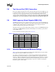
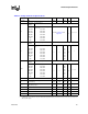
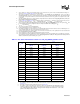
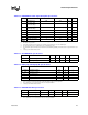
Table Of Contents
- Contents
- Revision History
- 1 Introduction
- 2 Electrical Specifications
- 2.1 FSB and GTLREF
- 2.2 Power and Ground Lands
- 2.3 Decoupling Guidelines
- 2.4 Voltage Identification
- 2.5 Reserved, Unused, and TESTHI Signals
- 2.6 FSB Signal Groups
- 2.7 GTL+ Asynchronous Signals
- 2.8 Test Access Port (TAP) Connection
- 2.9 FSB Frequency Select Signals (BSEL[2:0])
- 2.10 Absolute Maximum and Minimum Ratings
- 2.11 Processor DC Specifications
- 2.12 VCC Overshoot Specification
- 2.13 GTL+ FSB Specifications
- 3 Package Mechanical Specifications
- 4 Land Listing and Signal Descriptions
- 5 Thermal Specifications and Design Considerations
- 6 Features
- 7 Boxed Processor Specifications
- 8 Debug Tools Specifications

Datasheet 23
Electrical Specifications
2.8 Test Access Port (TAP) Connection
Due to the voltage levels supported by other components in the Test Access Port (TAP) logic, it is
recommended that the Celeron D processor in the 775-land package be first in the TAP chain and
followed by any other components within the system. A translation buffer should be used to
connect to the rest of the chain unless one of the other components is capable of accepting an input
of the appropriate voltage level. Similar considerations must be made for TCK, TMS, TRST#, TDI,
and TDO. Two copies of each signal may be required, with each driving a different voltage level.
2.9 FSB Frequency Select Signals (BSEL[2:0])
The BSEL[2:0] signals are used to select the frequency of the processor input clock (BCLK[1:0]).
Table 2-6 defines the possible combinations of the signals and the frequency associated with each
combination. The required frequency is determined by the processor, chipset, and clock
synthesizer. All agents must operate at the same frequency.
The Celeron D processor in the 775-land package currently operates at a 533 MHz FSB frequency
(selected by a 133 MHz BCLK[1:0] frequency). Individual processors will only operate at their
specified FSB frequency.
For more information about these signals, refer to Section 4.2.
2.10 Absolute Maximum and Minimum Ratings
Table 2-7 specifies absolute maximum and minimum ratings. Within functional operation limits,
functionality and long-term reliability can be expected.
At conditions outside functional operation condition limits, but within absolute maximum and
minimum ratings, neither functionality nor long-term reliability can be expected. If a device is
returned to conditions within functional operation limits after having been subjected to conditions
outside these limits, but within the absolute maximum and minimum ratings, the device may be
functional, but with its lifetime degraded depending on exposure to conditions exceeding the
functional operation condition limits.
Table 2-6. BSEL[2:0] Frequency Table for BCLK[1:0]
BSEL2 BSEL1 BSEL0 FSB Frequency
L L L Reserved
L L H 133 MHz
L H H Reserved
L H L Reserved
H L L Reserved
H L H Reserved
H H H Reserved
H H L Reserved