
Intel Celeron D Processor 300 Sequence
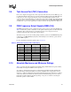
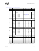
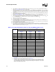
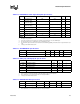
Table Of Contents
- Contents
- Revision History
- 1 Introduction
- 2 Electrical Specifications
- 2.1 FSB and GTLREF
- 2.2 Power and Ground Lands
- 2.3 Decoupling Guidelines
- 2.4 Voltage Identification
- 2.5 Reserved, Unused, and TESTHI Signals
- 2.6 FSB Signal Groups
- 2.7 GTL+ Asynchronous Signals
- 2.8 Test Access Port (TAP) Connection
- 2.9 FSB Frequency Select Signals (BSEL[2:0])
- 2.10 Absolute Maximum and Minimum Ratings
- 2.11 Processor DC Specifications
- 2.12 VCC Overshoot Specification
- 2.13 GTL+ FSB Specifications
- 3 Package Mechanical Specifications
- 4 Land Listing and Signal Descriptions
- 5 Thermal Specifications and Design Considerations
- 6 Features
- 7 Boxed Processor Specifications
- 8 Debug Tools Specifications
24 Datasheet
Electrical Specifications
At conditions exceeding absolute maximum and minimum ratings, neither functionality nor long-
term reliability can be expected. Moreover, if a device is subjected to these conditions for any
length of time then, when returned to conditions within the functional operating condition limits, it
will either not function, or its reliability will be severely degraded.
Although the processor contains protective circuitry to resist damage from static electric discharge,
precautions should always be taken to avoid high static voltages or electric fields.
2.11 Processor DC Specifications
The processor DC specifications in this section are defined at the processor core silicon and
not at the package lands unless noted otherwise. See Chapter 4 for the signal definitions and
signal assignments. Most of the signals on the processor FSB are in the GTL+ signal group. The
DC specifications for these signals are listed in Table 2-11.
Previously, legacy signals and Test Access Port (TAP) signals to the processor used low-voltage
CMOS buffer types. However, these interfaces now follow DC specifications similar to GTL+. The
DC specifications for these signal groups are listed in Table 2-10 and Table 2-12.
Table 2-8 through Table 2-14 list the DC specifications for the Celeron D processor in the 775-land
package and are valid only while meeting specifications for case temperature, clock frequency, and
input voltages. Care should be taken to read all notes associated with each parameter.
2.11.1 Processor DC Specifications
The processor DC specifications in this section are defined at the processor core silicon and
not at the package lands unless noted otherwise. See Chapter 4 for the signal definitions and
signal assignments. Most of the signals on the processor FSB are in the GTL+ signal group. The
DC specifications for these signals are listed in Table 2-10.
Table 2-8 through Table 2-15 list the DC specifications for the Celeron D processor in the 775-land
package and are valid only while meeting specifications for case temperature, clock frequency, and
input voltages. Care should be taken to read all notes associated with each parameter.
Table 2-7. Processor DC Absolute Maximum Ratings
Symbol Parameter Min Max Unit Notes
1, 2
NOTES:
1. For functional operation, all processor electrical, signal quality, mechanical and thermal specifications must be satisfied.
2. Excessive overshoot or undershoot on any signal will likely result in permanent damage to the processor.
V
CC
Core voltage with respect to
V
SS
- 0.3 1.55 V —
V
TT
FSB termination voltage with
respect to V
SS
- 0.3 1.55 V —
T
C
Processor case temperature See Chapter 5 See Chapter 5 °C —
T
STORAGE
Processor storage temperature –40 +85 °C
3, 4
3. Storage temperature is applicable to storage conditions only. In this scenario, the processor must not receive a clock, and
no lands can be connected to a voltage bias. Storage within these limits will not affect the long-term reliability of the device.
For functional operation, refer to the processor case temperature specifications.
4. This rating applies to the processor and does not include any tray or packaging.