
Intel Celeron D Processor 300 Sequence
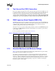
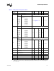
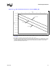
Table Of Contents
- Contents
- Revision History
- 1 Introduction
- 2 Electrical Specifications
- 2.1 FSB and GTLREF
- 2.2 Power and Ground Lands
- 2.3 Decoupling Guidelines
- 2.4 Voltage Identification
- 2.5 Reserved, Unused, and TESTHI Signals
- 2.6 FSB Signal Groups
- 2.7 GTL+ Asynchronous Signals
- 2.8 Test Access Port (TAP) Connection
- 2.9 FSB Frequency Select Signals (BSEL[2:0])
- 2.10 Absolute Maximum and Minimum Ratings
- 2.11 Processor DC Specifications
- 2.12 VCC Overshoot Specification
- 2.13 GTL+ FSB Specifications
- 3 Package Mechanical Specifications
- 4 Land Listing and Signal Descriptions
- 5 Thermal Specifications and Design Considerations
- 6 Features
- 7 Boxed Processor Specifications
- 8 Debug Tools Specifications
Datasheet 27
Electrical Specifications
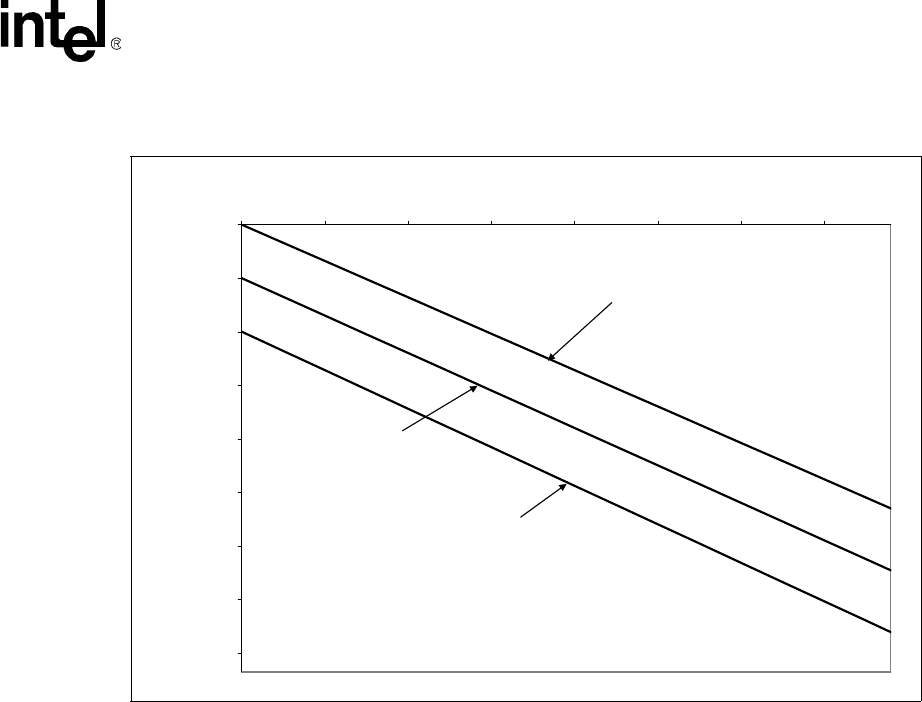
NOTES:
1. The loadline specification includes both static and transient limits except for overshoot allowed as shown in
Section 2.12.
2. This loadline specification shows the deviation from the VID set point.
3. The loadlines specify voltage limits at the die measured at the VCC_SENSE and VSS_SENSE lands. Voltage
regulation feedback for voltage regulator circuits must be taken from processor VCC and VSS lands. Refer to
the Voltage Regulator Down (VRD) 10.1 Design Guide For Desktop LGA775 Socket for socket loadline
guidelines and VR implementation details.
Figure 2-2. V
CC
Static and Transient Tolerance for 775_VR_CONFIG_04A
VID - 0.000
VID - 0.025
VID - 0.050
VID - 0.075
VID - 0.100
VID - 0.125
VID - 0.150
VID - 0.175
VID - 0.200
0 10203040506070
Icc [A]
Vcc [V]
Vcc Maximum
Vcc Typical
Vcc Minimum