
Intel Celeron D Processor 300 Sequence
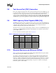
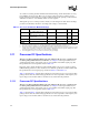
Table Of Contents
- Contents
- Revision History
- 1 Introduction
- 2 Electrical Specifications
- 2.1 FSB and GTLREF
- 2.2 Power and Ground Lands
- 2.3 Decoupling Guidelines
- 2.4 Voltage Identification
- 2.5 Reserved, Unused, and TESTHI Signals
- 2.6 FSB Signal Groups
- 2.7 GTL+ Asynchronous Signals
- 2.8 Test Access Port (TAP) Connection
- 2.9 FSB Frequency Select Signals (BSEL[2:0])
- 2.10 Absolute Maximum and Minimum Ratings
- 2.11 Processor DC Specifications
- 2.12 VCC Overshoot Specification
- 2.13 GTL+ FSB Specifications
- 3 Package Mechanical Specifications
- 4 Land Listing and Signal Descriptions
- 5 Thermal Specifications and Design Considerations
- 6 Features
- 7 Boxed Processor Specifications
- 8 Debug Tools Specifications
28 Datasheet
Electrical Specifications
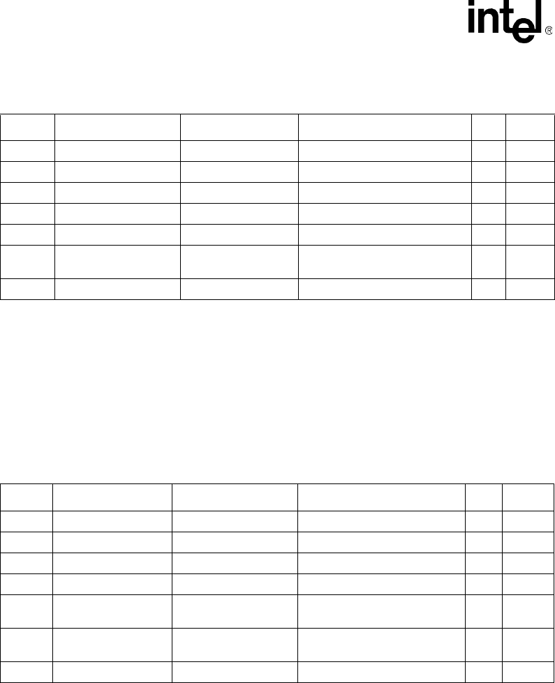
Table 2-10. GTL+ Asynchronous Signal Group DC Specifications
Symbol Parameter Min Max Unit Notes
1
NOTES:
1. Unless otherwise noted, all specifications in this table apply to all processor frequencies.
V
IL
Input Low Voltage 0.0 V
TT
/2 – (0.10 * V
TT
)—
2, 3
2. V
IL
is defined as the voltage range at a receiving agent that will be interpreted as a logical low value.
3. LINT0/INTR and LINT1/NMI use GTLREF as a reference voltage. For these two signals
V
IH
= GTLREF + (0.10 * VTT) and V
IL
= GTLREF – (0.10 * VTT).
V
IH
Input High Voltage V
TT
/2 + (0.10 * V
TT
)V
TT
—
3, 4, 5, 6
4. V
IH
is defined as the voltage range at a receiving agent that will be interpreted as a logical high value.
5. V
IH
and V
OH
may experience excursions above V
TT
.
6. The V
TT referred to in these specifications refers to instantaneous V
TT
.
V
OH
Output High Voltage 0.90*V
TT
V
TT
V
5, 6,
7
7. All outputs are open drain.
I
OL
Output Low Current — V
TT
/[(0.50*R
TT_MIN
) + R
ON_MIN
]A
8
8. The maximum output current is based on maximum current handling capability of the buffer and is not specified into the test
load.
I
LI
Input Leakage Current N/A ± 200 µA
9
9. Leakage to V
SS
with land held at V
TT
.
I
LO
Output Leakage
Current
N/A ± 200 µA
10
10. Leakage to V
TT
with land held at 300 mV.
R
ON
Buffer On Resistance 8 12 Ω
Table 2-11. GTL+ Signal Group DC Specifications
Symbol Parameter Min Max Unit Notes
1
NOTES:
1. Unless otherwise noted, all specifications in this table apply to all processor frequencies.
V
IL
Input Low Voltage 0.0 GTLREF – (0.10 * V
TT
)V
2, 3
2. V
IL
is defined as the voltage range at a receiving agent that will be interpreted as a logical low value.
3. The V
TT
referred to in these specifications is the instantaneous V
TT
.
V
IH
Input High Voltage GTLREF + (0.10 * V
TT
)V
TT
V
3, 4, 5
4. V
IH
is defined as the voltage range at a receiving agent that will be interpreted as a logical high value.
V
OH
Output High Voltage 0.90*V
TT
V
TT
V
3, 5
5. V
IH
and V
OH
may experience excursions above V
TT
.
I
OL
Output Low Current N/A V
TT
/[(0.50*R
TT_MIN
) + R
ON_MIN
]A -
I
LI
Input Leakage
Current
N/A ± 200 µA
6
6. Leakage to V
SS
with land held at V
TT
.
I
LO
Output Leakage
Current
N/A ± 200 µA
6
R
ON
Buffer On Resistance 8 12 Ω