
Intel Celeron D Processor 300 Sequence

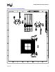
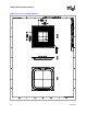
Table Of Contents
- Contents
- Revision History
- 1 Introduction
- 2 Electrical Specifications
- 2.1 FSB and GTLREF
- 2.2 Power and Ground Lands
- 2.3 Decoupling Guidelines
- 2.4 Voltage Identification
- 2.5 Reserved, Unused, and TESTHI Signals
- 2.6 FSB Signal Groups
- 2.7 GTL+ Asynchronous Signals
- 2.8 Test Access Port (TAP) Connection
- 2.9 FSB Frequency Select Signals (BSEL[2:0])
- 2.10 Absolute Maximum and Minimum Ratings
- 2.11 Processor DC Specifications
- 2.12 VCC Overshoot Specification
- 2.13 GTL+ FSB Specifications
- 3 Package Mechanical Specifications
- 4 Land Listing and Signal Descriptions
- 5 Thermal Specifications and Design Considerations
- 6 Features
- 7 Boxed Processor Specifications
- 8 Debug Tools Specifications
Datasheet 39
Package Mechanical Specifications
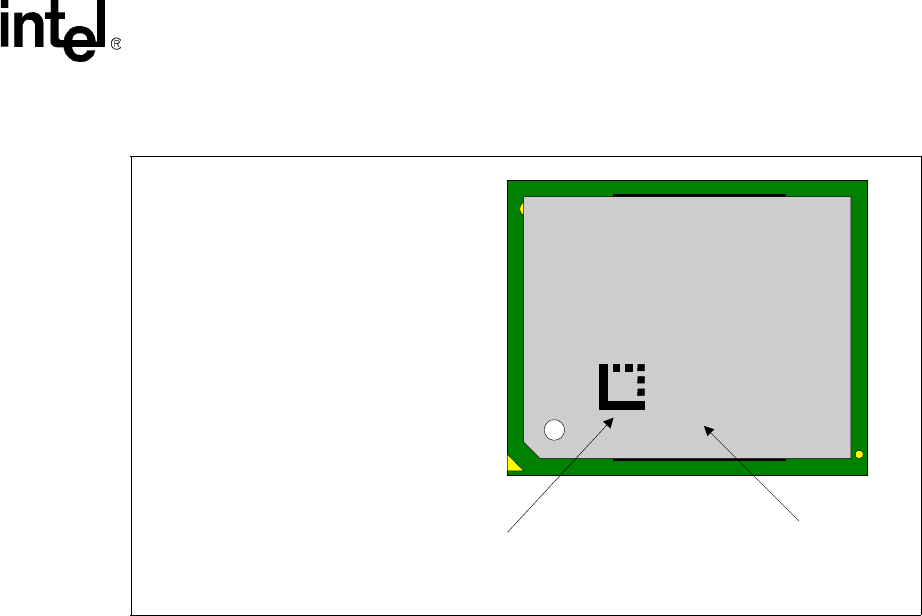
Figure 3-6. Processor Top-Side Marking Example
Grp1line1: INTEL m © ‘03
Grp1line2: CELERON® D
Grp1line3: 2.53GHZ/256/533
Grp1line4: SLxxx PHILLIPINES
Grp1line5: 7407A234
GROUP1 LINE1
GROUP1 LINE2
GROUP1 LINE3
GROUP1 LINE4
GROUP1 LINE5
ATPO #
SERIAL #
2D Matrix
ATPO #
SER #