
Intel Celeron D Processor 300 Sequence
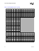
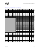
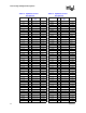
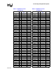
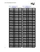


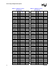
Table Of Contents
- Contents
- Revision History
- 1 Introduction
- 2 Electrical Specifications
- 2.1 FSB and GTLREF
- 2.2 Power and Ground Lands
- 2.3 Decoupling Guidelines
- 2.4 Voltage Identification
- 2.5 Reserved, Unused, and TESTHI Signals
- 2.6 FSB Signal Groups
- 2.7 GTL+ Asynchronous Signals
- 2.8 Test Access Port (TAP) Connection
- 2.9 FSB Frequency Select Signals (BSEL[2:0])
- 2.10 Absolute Maximum and Minimum Ratings
- 2.11 Processor DC Specifications
- 2.12 VCC Overshoot Specification
- 2.13 GTL+ FSB Specifications
- 3 Package Mechanical Specifications
- 4 Land Listing and Signal Descriptions
- 5 Thermal Specifications and Design Considerations
- 6 Features
- 7 Boxed Processor Specifications
- 8 Debug Tools Specifications

Datasheet 41
Land Listing and Signal Descriptions
4 Land Listing and Signal
Descriptions
This chapter contains the processor land assignments and signal descriptions.
4.1 Processor Land Assignments
This section contains the land listings for the Celeron D processor in the 775-land package. The
landout footprint is shown in Figure 4-1 and Figure 4-2. These figures show the physical location
of each signal on the package landout footprint (top view). Table 4-1 is a listing of all processor
lands ordered alphabetically by land (signal) name. Table 4-2 is also a listing of all processor lands;
the ordering is by land number.