
Intel Celeron D Processor 300 Sequence
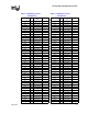
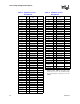

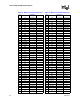
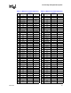
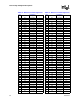

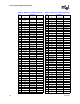

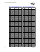
Table Of Contents
- Contents
- Revision History
- 1 Introduction
- 2 Electrical Specifications
- 2.1 FSB and GTLREF
- 2.2 Power and Ground Lands
- 2.3 Decoupling Guidelines
- 2.4 Voltage Identification
- 2.5 Reserved, Unused, and TESTHI Signals
- 2.6 FSB Signal Groups
- 2.7 GTL+ Asynchronous Signals
- 2.8 Test Access Port (TAP) Connection
- 2.9 FSB Frequency Select Signals (BSEL[2:0])
- 2.10 Absolute Maximum and Minimum Ratings
- 2.11 Processor DC Specifications
- 2.12 VCC Overshoot Specification
- 2.13 GTL+ FSB Specifications
- 3 Package Mechanical Specifications
- 4 Land Listing and Signal Descriptions
- 5 Thermal Specifications and Design Considerations
- 6 Features
- 7 Boxed Processor Specifications
- 8 Debug Tools Specifications

Land Listing and Signal Descriptions
Datasheet 53
Table 4-2. Numerical Land Assignments
Land
#
Land Name
Signal Buffer
Type
Direction
A2 VSS Power/Other —
A3 RS2# Common Clock Input
A4 D2# Source Synch Input/Output
A5 D4# Source Synch Input/Output
A6 VSS Power/Other —
A7 D7# Source Synch Input/Output
A8 DBI0# Source Synch Input/Output
A9 VSS Power/Other —
A10 D8# Source Synch Input/Output
A11 D9# Source Synch Input/Output
A12 VSS Power/Other —
A13 COMP0 Power/Other Input
A14 D50# Source Synch Input/Output
A15 VSS Power/Other —
A16 DSTBN3# Source Synch Input/Output
A17 D56# Source Synch Input/Output
A18 VSS Power/Other —
A19 D61# Source Synch Input/Output
A20 RESERVED — —
A21 VSS Power/Other —
A22 D62# Source Synch Input/Output
A23 VCCA Power/Other —
A24 VSS Power/Other —
A25 VTT Power/Other —
A26 VTT Power/Other —
A27 VTT Power/Other —
A28 VTT Power/Other —
A29 VTT Power/Other —
A30 VTT Power/Other —
B1 VSS Power/Other —
B2 DBSY# Common Clock Input/Output
B3 RS0# Common Clock Input
B4 D0# Source Synch Input/Output
B5 VSS Power/Other —
B6 D5# Source Synch Input/Output
B7 D6# Source Synch Input/Output
B8 VSS Power/Other —
B9 DSTBP0# Source Synch Input/Output
B10 D10# Source Synch Input/Output
B11 VSS Power/Other —
B12 D13# Source Synch Input/Output
B13 RESERVED — —
B14 VSS Power/Other —
B15 D53# Source Synch Input/Output
B16 D55# Source Synch Input/Output
B17 VSS Power/Other —
B18 D57# Source Synch Input/Output
B19 D60# Source Synch Input/Output
B20 VSS Power/Other —
B21 D59# Source Synch Input/Output
B22 D63# Source Synch Input/Output
B23 VSSA Power/Other —
B24 VSS Power/Other —
B25 VTT Power/Other —
B26 VTT Power/Other —
B27 VTT Power/Other —
B28 VTT Power/Other —
B29 VTT Power/Other —
B30 VTT Power/Other —
C1 DRDY# Common Clock Input/Output
C2 BNR# Common Clock Input/Output
C3 LOCK# Common Clock Input/Output
C4 VSS Power/Other —
C5 D1# Source Synch Input/Output
C6 D3# Source Synch Input/Output
C7 VSS Power/Other —
C8 DSTBN0# Source Synch Input/Output
C9 RESERVED — —
C10 VSS Power/Other —
C11 D11# Source Synch Input/Output
C12 D14# Source Synch Input/Output
C13 VSS Power/Other —
C14 D52# Source Synch Input/Output
C15 D51# Source Synch Input/Output
C16 VSS Power/Other —
C17 DSTBP3# Source Synch Input/Output
C18 D54# Source Synch Input/Output
C19 VSS Power/Other —
C20 DBI3# Source Synch Input/Output
C21 D58# Source Synch Input/Output
C22 VSS Power/Other —
C23 VCCIOPLL Power/Other —
C24 VSS Power/Other —
C25 VTT Power/Other —
C26 VTT Power/Other —
C27 VTT Power/Other —
C28 VTT Power/Other —
C29 VTT Power/Other —
Table 4-2. Numerical Land Assignments
Land
#
Land Name
Signal Buffer
Type
Direction