
Intel Celeron D Processor 300 Sequence
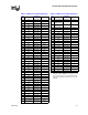
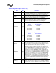
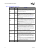
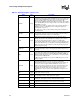
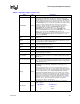
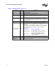
Table Of Contents
- Contents
- Revision History
- 1 Introduction
- 2 Electrical Specifications
- 2.1 FSB and GTLREF
- 2.2 Power and Ground Lands
- 2.3 Decoupling Guidelines
- 2.4 Voltage Identification
- 2.5 Reserved, Unused, and TESTHI Signals
- 2.6 FSB Signal Groups
- 2.7 GTL+ Asynchronous Signals
- 2.8 Test Access Port (TAP) Connection
- 2.9 FSB Frequency Select Signals (BSEL[2:0])
- 2.10 Absolute Maximum and Minimum Ratings
- 2.11 Processor DC Specifications
- 2.12 VCC Overshoot Specification
- 2.13 GTL+ FSB Specifications
- 3 Package Mechanical Specifications
- 4 Land Listing and Signal Descriptions
- 5 Thermal Specifications and Design Considerations
- 6 Features
- 7 Boxed Processor Specifications
- 8 Debug Tools Specifications
Land Listing and Signal Descriptions
Datasheet 61
AL20 VSS Power/Other —
AL21 VCC Power/Other —
AL22 VCC Power/Other —
AL23 VSS Power/Other —
AL24 VSS Power/Other —
AL25 VCC Power/Other —
AL26 VCC Power/Other —
AL27 VSS Power/Other —
AL28 VSS Power/Other —
AL29 VCC Power/Other —
AL30 VCC Power/Other —
AM1 VSS Power/Other —
AM2 VID0 Power/Other Output
AM3 VID2 Power/Other Output
AM4 VSS Power/Other —
AM5 VID6 Power/Other Output
AM6 VTTPWRGD Power/Other Input
AM7 VID7 Power/Other Output
AM8 VCC Power/Other —
AM9 VCC Power/Other —
AM10 VSS Power/Other —
AM11 VCC Power/Other —
AM12 VCC Power/Other —
AM13 VSS Power/Other —
AM14 VCC Power/Other —
AM15 VCC Power/Other —
AM16 VSS Power/Other —
AM17 VSS Power/Other —
AM18 VCC Power/Other —
AM19 VCC Power/Other —
AM20 VSS Power/Other —
AM21 VCC Power/Other —
AM22 VCC Power/Other —
AM23 VSS Power/Other —
AM24 VSS Power/Other —
AM25 VCC Power/Other —
AM26 VCC Power/Other —
AM27 VSS Power/Other —
AM28 VSS Power/Other —
AM29 VCC Power/Other —
AM30 VCC Power/Other —
AN1 VSS Power/Other —
AN2 VSS Power/Other —
AN3 VCC_SENSE Power/Other Output
Table 4-2. Numerical Land Assignments
Land
#
Land Name
Signal Buffer
Type
Direction
AN4 VSS_SENSE Power/Other Output
AN5
VCC_MB_
REGULATION
Power/Other Output
AN6
VSS_MB_
REGULATION
Power/Other Output
AN7 VID_SELECT Power/Other Output
AN8 VCC Power/Other —
AN9 VCC Power/Other —
AN10 VSS Power/Other —
AN11 VCC Power/Other —
AN12 VCC Power/Other —
AN13 VSS Power/Other —
AN14 VCC Power/Other —
AN15 VCC Power/Other —
AN16 VSS Power/Other —
AN17 VSS Power/Other —
AN18 VCC Power/Other —
AN19 VCC Power/Other —
AN20 VSS Power/Other —
AN21 VCC Power/Other —
AN22 VCC Power/Other —
AN23 VSS Power/Other —
AN24 VSS Power/Other —
AN25 VCC Power/Other —
AN26 VCC Power/Other —
AN27 VSS Power/Other —
AN28 VSS Power/Other —
AN29 VCC Power/Other —
AN30 VCC Power/Other —
NOTES:
1. EDRDY# and PC_REQ# are not features of the
Celeron D processor in the 775-land package.
They are included here for future processor com-
patibility.
Table 4-2. Numerical Land Assignments
Land
#
Land Name
Signal Buffer
Type
Direction