
Intel Celeron D Processor 300 Sequence
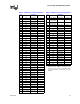
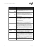
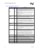
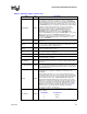
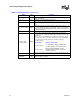
Table Of Contents
- Contents
- Revision History
- 1 Introduction
- 2 Electrical Specifications
- 2.1 FSB and GTLREF
- 2.2 Power and Ground Lands
- 2.3 Decoupling Guidelines
- 2.4 Voltage Identification
- 2.5 Reserved, Unused, and TESTHI Signals
- 2.6 FSB Signal Groups
- 2.7 GTL+ Asynchronous Signals
- 2.8 Test Access Port (TAP) Connection
- 2.9 FSB Frequency Select Signals (BSEL[2:0])
- 2.10 Absolute Maximum and Minimum Ratings
- 2.11 Processor DC Specifications
- 2.12 VCC Overshoot Specification
- 2.13 GTL+ FSB Specifications
- 3 Package Mechanical Specifications
- 4 Land Listing and Signal Descriptions
- 5 Thermal Specifications and Design Considerations
- 6 Features
- 7 Boxed Processor Specifications
- 8 Debug Tools Specifications

Datasheet 65
Land Listing and Signal Descriptions
DEFER# Input
DEFER# is asserted by an agent to indicate that a transaction cannot be
guaranteed in-order completion. Assertion of DEFER# is normally the
responsibility of the addressed memory or Input/Output agent. This signal
must connect the appropriate pins/lands of all processor FSB agents.
DP[3:0]#
Input/
Output
DP[3:0]# (Data Parity) provide parity protection for the D[63:0]# signals.
They are driven by the agent responsible for driving D[63:0]#, and must
connect the appropriate pins/lands of all processor FSB agents.
DRDY#
Input/
Output
DRDY# (Data Ready) is asserted by the data driver on each data transfer,
indicating valid data on the data bus. In a multi-common clock data
transfer, DRDY# may be de-asserted to insert idle clocks. This signal must
connect the appropriate pins/lands of all processor FSB agents.
DSTBN[3:0]#
Input/
Output
Data strobe used to latch in D[63:0]#.
DSTBP[3:0]#
Input/
Output
Data strobe used to latch in D[63:0]#.
EDRDY# Input
This signal indicates to the processor that the memory controller is about to
drive data on the bus based on a read request. The signal is driven from
the memory controller one BCLK[1:0] prior to data being driven on the bus.
EDRDY# is not a feature of the Celeron D processor in the 775-land
package. It is included here for future processor compatibility.
FERR#/PBE# Output
FERR#/PBE# (Floating Point Error/Pending Break Event) is a multiplexed
signal and its meaning is qualified by STPCLK#. When STPCLK# is not
asserted, FERR#/PBE# indicates a floating-point error and will be asserted
when the processor detects an unmasked floating-point error. When
STPCLK# is not asserted, FERR#/PBE# is similar to the ERROR# signal
on the Intel 387 coprocessor, and is included for compatibility with systems
using MS-DOS*-type floating-point error reporting. When STPCLK# is
asserted, an assertion of FERR#/PBE# indicates that the processor has a
pending break event waiting for service. The assertion of FERR#/PBE#
indicates that the processor should be returned to the Normal state. For
additional information on the pending break event functionality, including
the identification of support of the feature and enable/disable information,
refer to volume 3 of the Intel Architecture Software Developer's Manual and
the Intel Processor Identification and the CPUID Instruction application
note.
GTLREF[1:0] Input
GTLREF0 determines the signal reference level for GTL+ input signals.
GTLREF1 is not a feature of the Celeron D processor in the 775-Land
package. It is included here for future processor compatibility. GTLREF0 is
used by the GTL+ receivers to determine if a signal is a logical 0 or logical
1.
Table 4-3. Signal Description (Sheet 4 of 9)
Name Type Description
Signals Associated Strobe
D[15:0]#, DBI0# DSTBN0#
D[31:16]#, DBI1# DSTBN1#
D[47:32]#, DBI2# DSTBN2#
D[63:48]#, DBI3# DSTBN3#
Signals Associated Strobe
D[15:0]#, DBI0# DSTBP0#
D[31:16]#, DBI1# DSTBP1#
D[47:32]#, DBI2# DSTBP2#
D[63:48]#, DBI3# DSTBP3#