
Intel Celeron D Processor 300 Sequence
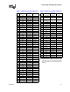
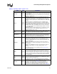
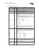
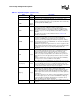
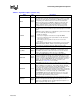
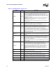
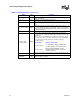
Table Of Contents
- Contents
- Revision History
- 1 Introduction
- 2 Electrical Specifications
- 2.1 FSB and GTLREF
- 2.2 Power and Ground Lands
- 2.3 Decoupling Guidelines
- 2.4 Voltage Identification
- 2.5 Reserved, Unused, and TESTHI Signals
- 2.6 FSB Signal Groups
- 2.7 GTL+ Asynchronous Signals
- 2.8 Test Access Port (TAP) Connection
- 2.9 FSB Frequency Select Signals (BSEL[2:0])
- 2.10 Absolute Maximum and Minimum Ratings
- 2.11 Processor DC Specifications
- 2.12 VCC Overshoot Specification
- 2.13 GTL+ FSB Specifications
- 3 Package Mechanical Specifications
- 4 Land Listing and Signal Descriptions
- 5 Thermal Specifications and Design Considerations
- 6 Features
- 7 Boxed Processor Specifications
- 8 Debug Tools Specifications

68 Datasheet
Land Listing and Signal Descriptions
RESET# Input
Asserting the RESET# signal resets the processor to a known state and
invalidates its internal caches without writing back any of their contents. For
a power-on Reset, RESET# must stay active for at least one millisecond
after V
CC
and BCLK have reached their proper specifications. On
observing active RESET#, all FSB agents will de-assert their outputs within
two clocks. RESET# must not be kept asserted for more than 10 ms while
PWRGOOD is asserted.
A number of bus signals are sampled at the active-to-inactive transition of
RESET# for power-on configuration. These configuration options are
described in the Section 6.1.
This signal does not have on-die termination and must be terminated on
the system board.
RS[2:0]# Input
RS[2:0]# (Response Status) are driven by the response agent (the agent
responsible for completion of the current transaction), and must connect
the appropriate pins/lands of all processor FSB agents.
RSP# Input
RSP# (Response Parity) is driven by the response agent (the agent
responsible for completion of the current transaction) during assertion of
RS[2:0]#, the signals for which RSP# provides parity protection. It must
connect to the appropriate pins/lands of all processor FSB agents.
A correct parity signal is high if an even number of covered signals are low
and low if an odd number of covered signals are low. While RS[2:0]# = 000,
RSP# is also high, since this indicates it is not being driven by any agent
guaranteeing correct parity.
SKTOCC# Output
SKTOCC# (Socket Occupied) will be pulled to ground by the processor.
System board designers may use this signal to determine if the processor
is present.
SMI# Input
SMI# (System Management Interrupt) is asserted asynchronously by
system logic. On accepting a System Management Interrupt, the processor
saves the current state and enter System Management Mode (SMM). An
SMI Acknowledge transaction is issued, and the processor begins program
execution from the SMM handler.
If SMI# is asserted during the de-assertion of RESET# the processor will
tristate its outputs.
STPCLK# Input
STPCLK# (Stop Clock), when asserted, causes the processor to enter a
low power Stop-Grant state. The processor issues a Stop-Grant
Acknowledge transaction, and stops providing internal clock signals to all
processor core units except the FSB and APIC units. The processor
continues to snoop bus transactions and service interrupts while in Stop-
Grant state. When STPCLK# is de-asserted, the processor restarts its
internal clock to all units and resumes execution. The assertion of
STPCLK# has no effect on the bus clock; STPCLK# is an asynchronous
input.
TCK Input
TCK (Test Clock) provides the clock input for the processor Test Bus (also
known as the Test Access Port).
TDI Input
TDI (Test Data In) transfers serial test data into the processor. TDI provides
the serial input needed for JTAG specification support.
TDO Output
TDO (Test Data Out) transfers serial test data out of the processor. TDO
provides the serial output needed for JTAG specification support.
TESTHI[13:0] Input
TESTHI[13:0] must be connected to a V
TT
power source through a resistor
for proper processor operation. See Section 2.5 for more details.
THERMDA Other Thermal Diode Anode. See Section 5.2.7.
THERMDC Other Thermal Diode Cathode. See Section 5.2.7.
Table 4-3. Signal Description (Sheet 7 of 9)
Name Type Description