
Intel Celeron D Processor 300 Sequence
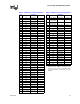
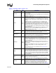
Table Of Contents
- Contents
- Revision History
- 1 Introduction
- 2 Electrical Specifications
- 2.1 FSB and GTLREF
- 2.2 Power and Ground Lands
- 2.3 Decoupling Guidelines
- 2.4 Voltage Identification
- 2.5 Reserved, Unused, and TESTHI Signals
- 2.6 FSB Signal Groups
- 2.7 GTL+ Asynchronous Signals
- 2.8 Test Access Port (TAP) Connection
- 2.9 FSB Frequency Select Signals (BSEL[2:0])
- 2.10 Absolute Maximum and Minimum Ratings
- 2.11 Processor DC Specifications
- 2.12 VCC Overshoot Specification
- 2.13 GTL+ FSB Specifications
- 3 Package Mechanical Specifications
- 4 Land Listing and Signal Descriptions
- 5 Thermal Specifications and Design Considerations
- 6 Features
- 7 Boxed Processor Specifications
- 8 Debug Tools Specifications
70 Datasheet
Land Listing and Signal Descriptions
§
VSS Input
VSS are the ground pins for the processor and should be connected to the
system ground plane.
VSSA Input VSSA is the isolated ground for internal PLLs.
VSS_SENSE Output
VSS_SENSE is an isolated low impedance connection to processor core
V
SS
. It can be used to sense or measure ground near the silicon with little
noise.
VSS_MB_REGULATION
Output
This land is provided as a voltage regulator feedback sense point for V
SS
. It
is connected internally in the processor package to the sense point land
V27 as described in the Voltage Regulator-Down (VRD) 10.1 Design Guide
for Desktop Socket 775.
VTT FSB termination voltage.
VTT_OUT_LEFT
VTT_OUT_RIGHT
Output
The VTT_OUT_LEFT and VTT_OUT_RIGHT signals are included to
provide a local V
TT
for some signals that require termination to V
TT
on the
motherboard.
For future processor compatibility some signals are required to be pulled
up to VTT_OUT_LEFT or VTT_OUT_RIGHT. Refer to the following table
for the signals that should be pulled up to VTT_OUT_LEFT and
VTT_OUT_RIGHT.
VTT_SEL Output
The VTT_SEL signal is used to select the correct V
TT
voltage level for the
processor.
VTTPWRGD Input
The processor requires this input to determine that the V
TT
voltages are
stable and within specification.
Table 4-3. Signal Description (Sheet 9 of 9)
Name Type Description
Pull Up Signal Signals to be Pulled Up
VTT_OUT_RIGHT
VTT_PWRGOOD, VID[5:0], GTLREF, TMS,
TDI, TDO, BPM[5:0], other VRD components
VTT_OUT_LEFT
RESET#, BR0#, PWRGOOD, TESTHI1,
TESTHI8, TESTHI9, TESTHI10, TESTHI11,
TESTHI12, TESTHI13