
Guide


I/O Subsystem
R
Intel
®
852GM Chipset Platform Design Guide 173
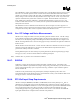
Table 71. Bus Capacitance Reference Chart
Device # of Devices/
Trace Length
Capacitance Includes Cap (pF)
ICH4-M 1 Pin Capacitance 12
CK408 1 Pin Capacitance 10
2 28 SO-
DIMMS
3
Pin Capacitance (10 pF) + 1 inch worth of trace capacitance (2 pF/inch)
per SO-DIMM and 2 pF connector capacitance per SO-DIMM
42
2 86
3 129
4 172
5 215
PCI
Slots
6
Each PCI add-in card is allowed up to 40 pF + 3 pF per each connector
258
≥24 48
≥36 72
Bus
Trace
Length
in inches
≥48
2 pF per inch of trace length
96
Table 72. Bus Capacitance/Pull-Up Resistor Relationship
Physical Bus Segment Capacitance Pull-Up Range (For Vcc = 3.3 V
0 to 100 pF 8.2 kΩ to 1.2 kΩ
100 to 200 pF 4.7 kΩ to 1.2 kΩ
200 to 300 pF 3.3 kΩ to 1.2 kΩ
300 to 400 pF 2.2 kΩ to 1.2 kΩ
10.7. FWH
The following provides general guidelines for compatibility and design recommendations for supporting
the FWH device. The majority of the changes will be incorporated in the BIOS. Refer to the
FWH
Datasheet
or equivalent.
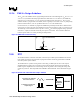
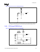
10.7.1. FWH Decoupling
Place a 0.1-µF capacitor between the V
CC
supply pins and the V
SS
ground pins to decouple high
frequency noise, which may affect the programmability of the device. Additionally, place a 4.7-µF
capacitor between the V
CC
supply pins and the V
SS
ground pins to decouple low frequency noise. The
capacitors should be placed no further than 390 mils from the V
CC
supply pins.