
Guide


I/O Subsystem
R
Intel
®
852GM Chipset Platform Design Guide 175
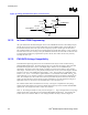
10.7.4. FWH V
PP
Design Guidelines
The V
PP
pin on the FWH is used for programming the flash cells. The FWH supports V
PP
of 3.3 V or 12
V. If
PP
is 12 V, the flash cells will program about 50% faster than at 3.3 V. However, the FWH only
supports 12 V V
PP
for 80 hours (3.3 V on Vpp does not affect the life of the device). The 12 V V
PP
would be useful in a programmer environment, which is typically an event that occurs very infrequently
(much less than 80 hours). The V
PP
pin MUST be tied to 3.3 V on the motherboard.
In some instances, it is desirable to program the FWH during assembly with the device soldered down
on the board. In order to decrease programming time it becomes necessary to apply 12 V to the V
PP
pin.
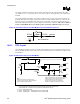
The following circuit will allow testers to put 12 V on the V
PP
pin while keeping this voltage separated
from the 3.3-V plane to which the rest of the power pins are connected. This circuit also allows the
board to operate with 3.3 V on this pin during normal operation.
Figure 89. FWH VPP Isolation Circuitry
1K
FET
12V (From Motherboard)3.3V
VPP
10.8. RTC
The ICH4-M contains a real time clock (RTC) with 256 bytes of battery backed SRAM. The internal
RTC module provides two key functions: keeping date and time and storing system data in its RAM
when the system is powered down.
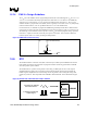
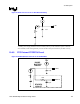
The ICH4-M uses a crystal circuit to generate a low-swing, 32-kHz input sine wave. This input is
amplified and driven back to the crystal circuit via the RTCX2 signal. Internal to the ICH4-M, the
RTCX1 signal is amplified to drive internal logic as well as generate a free running full swing clock
output for system use. This output ball of the ICH4-M is called SUSCLK. This is illustrated in Figure
90.
Figure 90. RTCX1 and SUSCLK Relationship in ICH4-M
ICH4-M
Internal
Oscillator
RTCX1
SUSCLK
Low-Swing 32.768 kHz
Sine Wave Source
Full-Swing 32.768 kHz
Output Signal