
Guide


I/O Subsystem
R
Intel
®
852GM Chipset Platform Design Guide 177
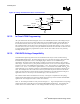
5. V
BIAS
: RTC BIAS Voltage – This ball is used to provide a reference voltage and this DC voltage sets a current,
which is mirrored throughout the oscillator and buffer circuitry.
6. V
SS
: Ground
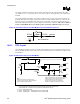
Table 73. RTC Routing Summary
RTC Routing
Requirements
Maximum Trace
Length To Crystal
Signal Length
Matching
R1, R2, C1, and C2
tolerances
Signal
Referencing
5 mil trace width
(results in ~2 pF per
inch)
1 inch NA R1 = R2 = 10 M
Ω ± 5%
C1 = C2 = (NPO class)
See Section
10.8.2 for
calculating a specific
capacitance value for C1
and C2.
Ground
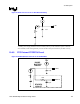
10.8.2. External Capacitors
To maintain the RTC accuracy, the external capacitor C
3
needs to be 0.047 µF and capacitor values C
1
and C
2
should be chosen to provide the manufacturer’s specified load capacitance (C
load
) for the crystal
when combined with the parasitic capacitance of the trace, socket (if used), and package. The following
equation can be used to choose the external capacitance values:
C
load
= [(C
1
+ C
in1
+ C
trace1
)*(C
2
+ C
in2
+ C
trace2
)]/[(C
1
+ C
in1
+ C
trace1
+ C
2
+ C
in2
+ C
trace2
)] + C
parasitic
Where:
• C
load
= Crystal’s load capacitance. This value can be obtained from Crystal’s specification.
• C
in1
, C
in2
= input capacitances at RTCX1, RTCX2 balls of the ICH4-M. These values can be
obtained in the
Intel
®
82801DBM I/O Controller Hub 4 Mobile (ICH4-M)I/O Controller Datasheet.
•
C
trace1
, C
trace2
= Trace length capacitances measured from Crystal terminals to RTCX1, RTCX2
balls. These values depend on the characteristics of board material, the width of signal traces and
the length of the traces. A typical value, based on a 5 mil wide trace and a ½ ounce copper pour, is
approximately equal to :
C
trace
= trace length * 2 pF/inch
• C
parasitic
= Crystal’s parasitic capacitance. This capacitance is created by the existence of two
electrode plates and the dielectric constant of the crystal blank inside the Crystal part. Refer to the
crystal’s specification to obtain this value.
Ideally, C
1
, C
2
can be chosen such that C
1
= C
2
. Using the equation of C
load
above, the value of C
1
, C
2
can be calculated to give the best accuracy (closest to 32.768 kHz) of the RTC circuit at room
temperature. However, C
2
can be chosen such that C
2
> C
1
. Then C
1
can be trimmed to obtain the
32.768 kHz.
In certain conditions, both C
1
, C
2
values can be shifted away from the theoretical values (calculated
values from the above equation) to obtain the closest oscillation frequency to 32.768 kHz. When C
1
, C
2
values are smaller then the theoretical values, the RTC oscillation frequency will be higher.
The following example will illustrates the use of the practical values C
1
, C
2
in the case that theoretical
values cannot guarantee the accuracy of the RTC in low temperature condition: