
Guide


I/O Subsystem
R
180 Intel
®
852GM Chipset Platform Design Guide
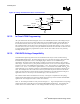
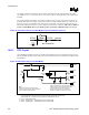
The ICH4-M RTC requires some additional external circuitry. The RTCRST# signal is used to reset the
RTC well. The external capacitor and the external resistor between RTCRST# and the RTC battery
(VBAT) were selected to create an RC time delay, such that RTCRST# will go high some time after the
battery voltage is valid. The RC time delay should be in the range of 18 ms - 25 ms. Any resistor and
capacitor combination that yields a time constant is acceptable. When RTCRST# is asserted, bit 2
(RTC_PWR_STS) in the GEN_PMCON_3 (General PM Configuration 3) register is set to 1, and
remains set until software clears it. As a result, when the system boots the BIOS knows that the RTC
battery has been removed.
This RTCRST# circuit is combined with the diode circuit (shown in Figure 93) whose purpose is to
allow the RTC well to be powered by the battery when the system power is not available. Figure 94 is an
example of this circuitry that is used in conjunction with the external diode circuit.
10.8.6. V
BIAS
DC Voltage and Noise Measurements
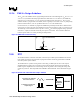
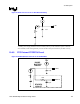
VBIAS is a DC voltage level that is necessary for biasing the RTC oscillator circuit. This DC voltage
level is filtered out from the RTC oscillation signal by the RC network of R2 and C3 (see Figure 92).
Therefore, it is a self-adjusting voltage. Board designers should not manually bias the voltage level on
VBIAS. Checking VBIAS level is used for testing purposes only to determine the right bias condition of
the RTC circuit.
VBIAS should be at least 200 mV DC. The RC network of R2 and C3 will filter out most of AC signal
noise that exists on this ball. However, the noise on this ball should be kept minimal in order to
guarantee the stability of the RTC oscillation.
Probing VBIAS requires the same technique as probing the RTCX1, RTCX2 signals (using Op-Amp).
See
Application Note AP-728 for further details on measuring techniques.
Note: VBIAS is also very sensitive to environmental conditions.
10.8.7. SUSCLK
SUSCLK is a square waveform signal output from the RTC oscillation circuit. Depending on the
quality of the oscillation signal on RTCX1 (largest voltage swing), SUSCLK duty cycle can be between
30-70%. If the SUSCLK duty cycle is beyond 30-70% range, it indicates a poor oscillation signal on
RTCX1 and RTCX2.
SUSCLK can be probed directly using normal probe (50-
Ω input impedance probe) and it is an
appropriated signal to check the RTC frequency to determine the accuracy of the ICH4-M’s RTC Clock
(see
Application Note AP-728 for further details).
10.8.8. RTC-Well Input Strap Requirements
All RTC-well inputs (RSMRST#, RTCRST#, INTRUDER#) must be either pulled up to V
CC
RTC or
pulled-down to ground while in the G3 state. RTCRST# when configured as shown in Figure 94 meets
this requirement. RSMRST# should have a weak external pull-down to ground and INTRUDER# should
have a weak external pull-up to V
CC
RTC. This will prevent these nodes from floating in G3, and
correspondingly will prevent I
CC
RTC leakage that can cause excessive coin-cell drain. The PWROK
input signal should also be configured with an external weak pull-down.