
Guide


Platform Clock Routing Guidelines
R
Intel
®
852GM Chipset Platform Design Guide 197
11. Platform Clock Routing Guidelines
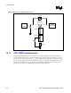
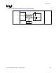
11.1. System Clock Groups
The system clocks are considered as a subsystem in themselves. At the center of this subsystem is the
Clock Synthesizer/Driver component. Several vendors offer suitable products, as defined in the Intel
CK408 Synthesizer/Driver Specification. This device provides the set of clocks required to implement a
platform level motherboard solution. Table 78 below provides a breakdown of the various individual
clocks.
Note: When used in Intel 852GM platforms the CK408 is configured in the unbuffered mode and a host clock
swing of 710 mV.
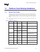
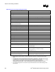
Table 78. Individual Clock Breakdown
Clock Group Frequency Driver/Pin Receiver/s Comments
HOST_CLK 100 MHz CK408
CPU[2:0]
CPU
GMCH
Debug Port
Length matched
Differential signaling
CLK66 66 MHz CK408
3V66[5:0]
GMCH
ICH4-M
Length matched
33MHz CK408
PCIF[2:0]
ICH4-M CLK33
33 MHz CK408
PCI[6:0]
SIO
FWH
Length matched to CLK66
Synchronous but not edge aligned with
CLK66
Phase delay of 1.5 ns to 3.5 ns
PCICLK
(Expansion)
33 MHz CK408
PCI[6:0]
PCI Conn #1
PCI Conn #2
PCI Conn #3
Length matched to CLK33 *
* CLK33 length minus 2.5”
CLK14 14 MHz CK408
REF0
ICH4-M
SIO
Independent clock
DOTCLK 48 MHz
CK408
48 MHz
GMCH Independent clock
SSCCLK 48/66 MHz CK408
VCH
GMCH Independent clock
USBCLK 48 MHz
CK408
48 MHz
ICH4-M Independent clock