
Design Guide

System Memory Design Guidelines (DDR-SDRAM) for SO-DIMM configuration
R
112 Intel
®
855GM/855GME Chipset Platform Design Guide
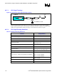
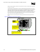
6.3.7.1. CPC Signal Topology
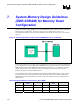
Figure 50. Command per Clock Signal Routing Topology
P1
Vtt
SO-DIMM0,1 PAD
w
Rt
L2
GMCH
Pin
GMCH
L1
S1
The CPC signals should be routed using 2 to 1 trace space to width ratio for signals within the DDR
group, except clocks and strobes. There should be a minimum of 20-mils of spacing to non-DDR related
signals. CPC signals should be routed on inner layers with minimized external trace lengths.
6.3.7.2. CPC Signal Routing Guidelines
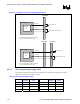
Table 37. CPC Signal Routing Guidelines
Parameter Routing Guidelines
Signal Group SMA[5,4,2,1], SMAB[5,4,2,1]
Motherboard Topology Point-to-Point with Parallel Termination
Reference Plane Ground Referenced
Characteristic Trace Impedance (Zo) 55 Ω ±15%
Nominal Trace Width
Inner layers: 4 mils
Outer layers: 5 mils
Minimum Spacing to Trace Width Ratio 2 to 1 (e.g. 8 mil space to 4 mil trace)
Minimum Isolation Spacing to non-DDR Signals 20 mils
Package Length P1
500 mils +/- 250 mils
(See Table 38 for exact package lengths.)
Stub Length S1 Max = 0.25”
Trace Length L1 – GMCH Control Signal Ball to SO-DIMM Pad
Min = 0.5 inches
Max = 5.5 inches for DDR266
Max = 4.5 inches for DDR333
Trace Length L2 – SO-DIMM Via to Parallel Termination Resistor
Pad
Max = 2.0 inches
Parallel Termination Resistor (Rt) 56 Ω ± 5%
Maximum Recommended Motherboard Via Count Per Signal 3