
Design Guide

System Memory Design Guidelines (DDR-SDRAM) for SO-DIMM configuration
R
114 Intel
®
855GM/855GME Chipset Platform Design Guide
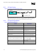
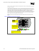
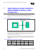
Figure 51. CPC Signals to Clock Length Matching Diagram
SO-DIMM0
GMCH Package
SMA[5,4,2,1]
SCK[2:0]
SCK#[2:0]
Note: All lengths are measured from GMCH
die pad to SO-DIMM connector pad.
CPC Length = Y0
Clock Reference Length = X0
SO-DIMM0 SO-DIMM1
SCK[5:3]
SCK#[5:3]
Clock Ref Length = X1
Note: All lengths are measured from GMCH
die pad to SO-DIMM connector pad.
SMAB[5,4,2,1]
CPC Length = Y1
GMCH Package
GMCH
Die
GMCH
Die
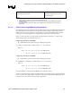
6.3.7.4. CPC Group Package Length Table
The package length data in the table below should be used to match the overall length of each CPC
signal to it’s associated clock reference length.
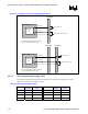
Table 38. CPC Group Package Lengths
Signal
Pin
Number
Pkg Length
(mils)
Signal
Pin
Number
Pkg Length
(mils)
SMA[1] AD14 398 SMAB[1] AD16 427
SMA[2] AD13 443 SMAB[2] AC12 395
SMA[4] AD11 430 SMAB[4] AF11 716
SMA[5] AC13 346 SMAB[5] AD10 631