
Design Guide

System Memory Design Guidelines (DDR-SDRAM) for Memory Down Configuration
R
122 Intel
®
855GM/855GME Chipset Platform Design Guide
7.1. Length Matching and Length Formulas
The routing guidelines presented in the following subsections define the recommended routing
topologies, trace width, spacing geometries, and absolute minimum and maximum routed lengths for
each signal group. These parameters are recommended to achieve optimal SI and timing. In addition to
the absolute length limits provided in the individual guideline tables, more restrictive length matching
formulas are also provided. These formulas further restrict the minimum to maximum length range of
each signal group with respect to clock, within the overall boundaries defined in the guideline tables, as
required to guarantee adequate timing margins. These secondary constraints are referred to as length
matching constraints and the formulas used are referred to as length matching formulas.
All signal groups, except feedback signals, are length matched to the DDR clocks. The clocks on a given
Micro-DIMM or memory down configuration are length matched to within ± 25 mils of the target
length. A different clock target length may be used for each Micro-DIMM. The difference in clock
target lengths between Micro-DIMM and Memory Down should not exceed 2 inches. A simple
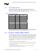
summary of the length matching formulas for each signal group is provided in Table 42
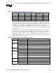
Table 42. Length Matching Formulas
Signal Group Minimum Length Maximum Length
Control to Clock Clock –1.0” Clock + 0.5”
Command to Clock Clock – 2.0” Clock + 2.0”
CPC to Clock Clock – 1.0” Clock + 0.5”
Strobe to Clock Clock – 2.0” Clock + 0.5”
Data to Strobe Strobe – 25 mils Strobe + 25 mils
Note: All length matching formulas are based on GMCH die-pad to Micro-DIMM connector pad or Memory
Down device pin total length.
Package length tables are provided for all signals in order to facilitate this pad-to-pin matching. The
clock lengths to Memory Down may be up to 2 inches longer than the clock lengths to the Micro-
DIMM. Length formulas should be applied to Micro-DIMM and Memory Down separately. The full
geometry and routing guidelines along with the exact length matching formulas and associated diagrams
are provided in the individual signal group guidelines sections.
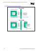
7.2. Package Length Compensation
As mentioned in Section 7.1, all length matching is done from the GMCH die-pad to Micro-DIMM
connector pad or memory device pin. The reason for this is to compensate for the package length
variation across each signal group. The GMCH does not equalize package lengths internally as some
previous GMCH components have, and therefore, the 855GM/GME GMCH requires length matching.
Package length compensation should not be confused with length matching as discussed in the previous
section. Length matching refers to constraints on the min and max length bounds of a signal group
based on clock length, whereas package length compensation refers to the process of adjusting out
package length variance across a signal group. There is of course some overlap in that both affect the
target length of an individual signal. Intel recommends that the initial route be completed based on the