
Design Guide

System Memory Design Guidelines (DDR-SDRAM) for Memory Down Configuration
R
Intel
®
855GM/855GME Chipset Platform Design Guide 123
length matching formulas in conjunction with nominal package lengths and that package length
compensation be performed as a secondary operation.
7.3. Topologies and Routing Guidelines
The 855GM/GME GMCH chipset’s Double Data Rate (DDR) SDRAM system memory interface
implements the low swing, high-speed, terminated SSTL_2 topology. This section contains information
related to the recommended interconnect topologies and routing guidelines for each of the signal groups
which comprise the DDR interface. When implemented as defined, these guidelines will provide for a
robust DDR solution on a 855GM/GME GMCH chipset based design..
7.3.1. Clock Signals – SCK[4,3,1,0], SCK#[4,3,1,0]
The clock signal group includes the differential clock pairs SCK/SCK#[4,3,1,0]. SCK/SCK#[5,2] are
not used for this configuration and are not connected on the motherboard. The GMCH generates and
drives these differential clock signals required by the DDR interface; therefore, no external clock driver
is required for the DDR interface. The GMCH supports unbuffered DDR Micro-DIMM; two differential
clock pairs are routed to the Micro-DIMM connector and two to the Memory Down configuration.
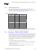
Table 43 summarizes the clock signal mapping.
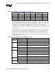
Table 43. Clock Signal Mapping
Signal Relative To
SCK/SCK#[1:0] Micro-DIMM
SCK/SCK#[4:3] Memory Down
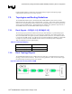
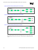
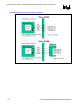
7.3.2. Clock Topology Diagram
The 855GM/GME GMCH provides 6 differential clock output pairs. The motherboard clock routing
topology is shown below for reference. Refer to the routing guidelines in Table 44 on the follow page
for detailed length and spacing rules for each segment.
Figure 54. DDR Clock Routing to Micro-DIMM