
Design Guide

System Memory Design Guidelines (DDR-SDRAM) for Memory Down Configuration
R
124 Intel
®
855GM/855GME Chipset Platform Design Guide
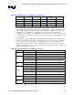
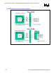
Figure 55. DDR Clock Routing to Memory Down Two Load BGA
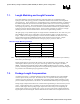
Figure 56. DDR Clock Routing to Memory Down Two Load TSOP
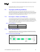
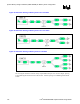
Figure 57. DDR Clock Routing to Memory Down 4 Load BGA
The clock signals should be routed as closely coupled differential pairs over the entire length. Spacing
to other DDR signals should not be less than 20 mils. Isolation spacing to non-DDR signals should be
25 mils.